
Page 309 - Book Hosokawa Nanoparticle Technology Handbook
P. 309
FUNDAMENTALS CH. 5 CHARACTERIZATION METHODS FOR NANOSTRUCTURE OF MATERIALS
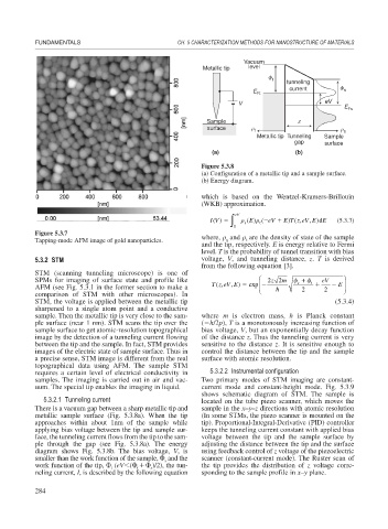
Vacuum
Metallic tip level
t
tunneling
current
E Ft s
V eV
E
Fs
Sample z
surface t s
Metallic tip Tunneling Sample
gap surface
(a) (b)
Figure 5.3.8
(a) Configuration of a metallic tip and a sample surface.
(b) Energy diagram.
which is based on the Wentzel-Kramers-Brillouin
(WKB) approximation.
∫ eV
IV() s ( E) ( eV E T z eV E)d E (5.3.3)
(
)
,
,
t
0
Figure 5.3.7
s
t
Tapping-mode AFM image of gold nanoparticles. where, and are the density of state of the sample
and the tip, respectively. E is energy relative to Fermi
level. T is the probability of tunnel transition with bias
5.3.2 STM voltage, V, and tunneling distance, z. T is derived
from the following equation [3].
STM (scanning tunneling microscope) is one of
SPMs for imaging of surface state and profile like ⎛ z 2 2m + t eV ⎞
s
⎜
,
(,
AFM (see Fig. 5.3.1 in the former section to make a Tz eV E) exp 2 2 E ⎟ ⎠
⎝
comparison of STM with other microscopes). In
STM, the voltage is applied between the metallic tip (5.3.4)
sharpened to a single atom point and a conductive
sample. Then the metallic tip is very close to the sam- where m is electron mass, h is Planck constant
ple surface (near 1 nm). STM scans the tip over the ( h/2p), T is a monotonously increasing function of
sample surface to get atomic-resolution topographical bias voltage, V, but an exponentially decay function
image by the detection of a tunneling current flowing of the distance z. Thus the tunneling current is very
between the tip and the sample. In fact, STM provides sensitive to the distance z. It is sensitive enough to
images of the electric state of sample surface. Thus in control the distance between the tip and the sample
a precise sense, STM image is different from the real surface with atomic resolution.
topographical data using AFM. The sample STM
requires a certain level of electrical conductivity in 5.3.2.2 Instrumental configuration
samples. The imaging is carried out in air and vac- Two primary modes of STM imaging are constant-
uum. The special tip enables the imaging in liquid. current mode and constant-height mode. Fig. 5.3.9
shows schematic diagram of STM. The sample is
5.3.2.1 Tunneling current located on the tube piezo scanner, which moves the
There is a vacuum gap between a sharp metallic tip and sample in the x–y–z directions with atomic resolution
metallic sample surface (Fig. 5.3.8a). When the tip (In some STMs, the piezo scanner is mounted on the
approaches within about 1nm of the sample while tip). Proportional-Integral-Derivative (PID) controller
applying bias voltage between the tip and sample sur- keeps the tunneling current constant with applied bias
face, the tunneling current flows from the tip to the sam- voltage between the tip and the sample surface by
ple through the gap (see Fig. 5.3.8a). The energy adjusting the distance between the tip and the surface
diagram shows Fig. 5.3.8b. The bias voltage, V, is using feedback control of z voltage of the piezoelectric
smaller than the work function of the sample, and the scanner (constant-current mode). The Ruster scan of
s
work function of the tip, (eV ( )/2), the tun- the tip provides the distribution of z voltage corre-
t
t
s
neling current, I, is described by the following equation sponding to the sample profile in x–y plane.
284