
Page 311 - Book Hosokawa Nanoparticle Technology Handbook
P. 311
FUNDAMENTALS CH. 5 CHARACTERIZATION METHODS FOR NANOSTRUCTURE OF MATERIALS
pull away Etching
intersection
point of wire cutting tip Stainless tube tip
and blade wire cutter surface
blade of
Pt/Ir wire
45°
tunneling Pt ring tunneling
point point
tunneling tunneling
Pt/Ir wire sample surface current current
sample surface
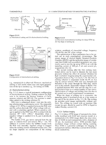
Figure 5.3.11
(a) Mechanical cutting and (b) electrochemical etching. Figure 5.3.13
(a) Precision electrochemical etching for sharp STM tip.
(b) Tip shape of etching tip.
Current
monitor Teflon
micrometer solution, amplitude of sinusoidal voltage, frequency
screw
Bipolar (50–60 Hz) and DC offset voltage.
amplifier The optimization of these parameters has to be car-
ried out in each experimental circumstance. The
Function atomic image of cleaved Highly Oriented Pyrolytic
generator Graphite (HOPG) and the molecular image of octade-
Stainless
tube cane thiol SAM (self-assembled monolayer) are com-
monly used to test the tip using STM in air with the
tunneling current of 100 pA–1 nA and several pA,
Pt/Ir wire respectively [10, 11].
Carbon electrode The second etching after the first etching men-
tioned above can be used to sharpen the tips more
precisely without the effect of external vibration for
Figure 5.3.12 high resolution imaging using the experimental con-
Configuration of electrochemical etching.
figuration shown in Fig. 5.3.13a [4, 7, 9]. The film of
etching solution is suspended inside the Pt (or Au)
ring by surface tension. Pt/Ir wire was clamped and
e.g., nanoparticle is observed. However, mechanical threaded at the center through the Pt/Ir ring, which
cutting is still useful when easy and rapid prepara- acts as the cathode. Sinusoidal voltage of about 2 Vac
tion of the tip is needed, e.g., for testing of STM.
is applied between Pt/Ir wire and the ring for a cer-
(3) Electrochemical etching tain period of time or a certain number of sine waves.
Optimization of voltage and etching time also has to
Fig. 5.3.12 shows a typical instrument configuration be carried out in each experimental circumstance.
of electrochemical etching. Etching solution for Pt/Ir When the shape of etching tip is symmetric, the
wire is for instance the mixture solution of CaCl 2 tunneling point is localized at one or a few atoms at
aqueous solution and HCl [4]. The acetone is some- the end of the tip shown in Fig. 5.3.13b. The etching
times added to the etching solution [5]. tip provides good image reproducibly without arti-
Pt/Ir wire is submerged about 1 mm into the etch-
ing solution using a micrometer screw. The sinusoidal facts. The etching tip coated with an insulator film
except tip apex should be used for STM in liquid to
voltage of 25–50 Vac is applied between the Pt/Ir wire reduce Faraday current [12].
and the carbon electrode (DC offset voltage with sev-
eral volt is sometimes applied). When a positive volt-
age is applied to the Pt/Ir wire, Pt/Ir is etched with the 5.3.2.4 Surface imaging
4
reaction. Pt 6Cl PtCl 6 2 Meanwhile when a Fig. 5.3.14 shows STM image of nanoparticles chem-
negative voltage is applied to it, H gas is produced, ically modified with SAM and structure model of a
2
2H 2e H . nanoparticle [13]. STM image shows the clear struc-
2
The bubble of H gas moves upward from the tip ture of SAM on each nanoparticle with a diameter of
2
apex to solution level and remove PtCl 6 2 ion. The 10 nm. As mentioned above, STM provides high-
addition of acetone makes the bubbles escape from resolution image without contact during scanning.
the Pt/Ir wire smoothly. Applied voltage is stopped Thus STM is a powerful technique for imaging of
when the etching current measured reaches zero. The nanoparticle surface, which has a certain level of elec-
tip shape depends on composition of the etching trical conductivity.
286