
Page 316 - Book Hosokawa Nanoparticle Technology Handbook
P. 316
5.3 SURFACE STRUCTURE FUNDAMENTALS
energy of h , in which h is Planck constant and is by diffracting and focusing a non-monochromatic K
frequency of the radiation, the photon energy is totally X-ray radiation emitted from an electron-bombarded
absorbed by an electron that is bound in either core thin metal anode (usually Mg or Al), which gives rise
levels or valence levels of an atom in a molecule or to MgK radiation with a photon energy of 1253.6 eV
solid with a binding energy of E , leading to ioniza- and AlK radiation with a photon energy of 1486.6
b
tion and the emission of the bound electron out of the eV. Photoelectrons, which are emitted from the sam-
atom with an energy of h E through the photo- ple surface through the photoelectric effect, are col-
b
electric effect. Hence, the photo-emitted electron is lected into the electron energy analyzer. There exist a
called a photoelectron. variety of designs for the electron analyzer, however,
Now let us consider a physical situation to measure the most preferred and the most commonly employed
an energy spectrum of photoelectrons emitted from a design for the photoelectron spectroscopy is a con-
solid-material sample, which is irradiated with a centric hemispherical analyzer, in which a static elec-
monochromatic soft X-ray radiation beam, using an tric field between two hemispherical surfaces
electron energy analyzer that is electrically con- disperses electrons according to their kinetic energy.
nected to the solid–material sample, as schematically The energy-analyzed electrons are normally detected
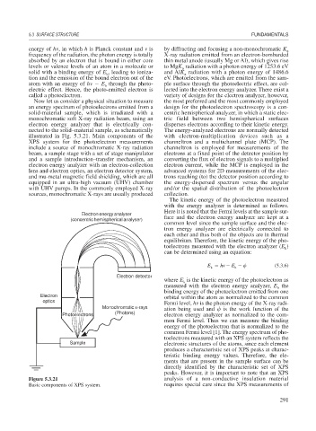
illustrated in Fig. 5.3.21. Main components of the with electron-multiplication devices such as a
XPS system for the photoelectron measurements channeltron and a multichannel plate (MCP). The
include a source of monochromatic X-ray radiation channeltron is employed for measurements of the
beam, a sample stage with a set of stage manipulator electrons at a fixed point of the detector position by
and a sample introduction–transfer mechanism, an converting the flux of electron signals to a multiplied
electron energy analyzer with an electron-collection electron current, while the MCP is employed in the
lens and electron optics, an electron detector system, advanced systems for 2D measurements of the elec-
and mu-metal magnetic field shielding, which are all trons reaching (to) the detector position according to
equipped in an ultra-high vacuum (UHV) chamber the energy-dispersed spectrum versus the angular
with UHV pumps. In the commonly employed X-ray and/or the spatial distribution of the photoelectron
sources, monochromatic X-rays are usually produced collection.
The kinetic energy of the photoelectron measured
with the energy analyzer is determined as follows.
Here it is noted that the Fermi levels at the sample sur-
Electron energy analyser
(concentric hemispherical analyser) face and the electron energy analyzer are kept at a
common level since the sample surface and the elec-
tron energy analyzer are electrically connected to
each other and thus both of the objects are in thermal
equilibrium. Therefore, the kinetic energy of the pho-
toelectrons measured with the electron analyzer (E )
k
can be determined using an equation:
E h E (5.3.6)
k b
Electron detector
where E is the kinetic energy of the photoelectron as
k
measured with the electron energy analyzer, E the
b
binding energy of the photoelectron emitted from one
Electron orbital within the atom as normalized to the common
optics
Fermi level, h is the photon energy of the X-ray radi-
Monochromatic x-rays ation being used and is the work function of the
Photoelectrons (Photons) electron energy analyzer as normalized to the com-
mon Fermi level. Thus we can measure the binding
energy of the photoelectron that is normalized to the
common Fermi level [1]. The energy spectrum of pho-
toelectrons measured with an XPS system reflects the
Sample electronic structures of the atoms, since each element
produces a characteristic set of XPS peaks at charac-
teristic binding energy values. Therefore, the ele-
ments that are present in the sample surface can be
directly identified by the characteristic set of XPS
peaks. However, it is important to note that an XPS
Figure 5.3.21 analysis of a non-conductive insulation material
Basic components of XPS system. requires special care since the XPS measurements of
291