
Page 318 - Book Hosokawa Nanoparticle Technology Handbook
P. 318
5.3 SURFACE STRUCTURE FUNDAMENTALS
with the conventional XPS system can be performed escape into the vacuum without suffering significant
by properly selecting the X-ray energy and the elec- energy loss, while the electrons that originated in rela-
tron escape angle. tively deeper regions are considered to form tails and
In routine analysis by XPS, two kinds of spectrum- background of the XPS spectrum in the lower kinetic
survey modes are usually taken in scanning the kinetic energy region (i.e., higher binding-energy region in
energy by properly setting the energy width and the res- the spectrum). In addition, it is shown that the signals
olution for measurements; (a) wide-scan survey spec- for boron, carbon, and nitrogen, which are the neigh-
trum (wide energy width and low energy resolution; bor elements in the periodic table, are clearly discrim-
mainly employed for qualitative analysis of elements) inated in the spectrum.
and (b) narrow-scan survey spectrum (narrow energy In the narrow-scan survey spectrum shown in
width and high energy resolution; mainly employed for Fig. 5.3.25, which is measured for photoelectrons
quantitative analysis of elemental composition and for emitted from the C1s orbital, in this example, it is eval-
analysis of chemical state identification). uated that the chemical bonding state of carbon atoms
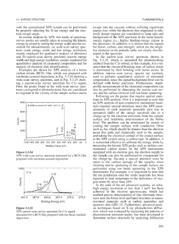
Examples are shown for XPS analysis of a boron is dominated by their bonding with boron atoms. In
carbon nitride (BCN) film, which was prepared with addition, narrow-scan survey spectra are routinely
ion-beam-assisted deposition, in Fig. 5.3.24 showing a used to perform quantitative analysis of elemental
wide-scan survey spectrum, and in Fig. 5.3.25 show- composition, since the signal background level can be
ing a narrow-scan survey spectrum for C1s signal. defined with better precision. Furthermore, depth-
First, the peaks found in the wide-scan survey spec- profile measurements of the elemental composition can
trum correspond to photoelectrons that are considered also be performed by alternating the narrow-scan sur-
to originate in the vicinity of the sample surface and to vey and the surface removal with ion-beam sputtering.
Following are the points that require special atten-
tions in XPS analysis. First it is important to note that
8000 an XPS analysis of non-conductive (insulation) mate-
N 1s
BCN film prepared with IBAD (5at% C) rials requires special attentions since the XPS meas-
urements of such materials generally give rise to
6000 unwanted shifts of the energy spectrum due to a
charge-up by the electron emissions from the sample
Counts 4000 surface and indefinite determination of the Fermi
level. The problem can be minimized by means of
O 1s N sat B 1s coating the sample surface with conductive films
such as Au, which should be thinner than the electron
2000 Ar 2p B Sat
Ar 2s C 1s mean free path and chemically inert to the sample,
and taking the electrical contact of the coated surface
to the XPS system using a carbon tape. In addition, it
0
11001000 900 800 700 600 500 400 300 200 100 0 is somewhat effective to calibrate the energy shifts by
Binding Energy (eV) measuring the known XPS peaks such as surface con-
taminated carbon atoms. In the XPS instruments
Figure 5.3.24 equipped with an electron gun, the electron supply to
XPS wide-scan survey spectrum measured for a BCN film the sample can also be performed to compensate for
prepared with ion-beam-assisted deposition. the charge-up. Second, a special attention must be
taken to the surface damage of the samples when
cleaning and/or sputtering of the sample surface are
1000 performed using ion beam sputtering in the XPS
C1s instruments. For example, it is important to note that
C-B the ion irradiation onto the oxide materials has been
Counts C-N C-C reported to lead sometimes to the deficiency of oxy-
gen atoms by more than 10%.
In the state-of-the-art advanced systems, an ultra-
C-O high energy resolution of less than 1 meV has been
achieved in the electron spectroscopy, which has
enabled precise determination of fine electronic struc-
291.0 287.8 284.6 281.4 278.2 275.0 tures near the Fermi level and band structures in nanos-
Binding Energy (eV) tructured materials such as carbon nanotubes and
quantum dots (QD) [4]. Furthermore, advanced analy-
Figure 5.3.25 sis techniques based on X-ray photoelectron diffrac-
XPS narrow-scan survey spectrum for C1s signal tion, which was evaluated by measuring the patterns of
measured for a BCN film prepared with ion-beam-assisted photoelectron emission angles, has been developed to
deposition. determine surface structures by analyzing diffraction
293