
Page 374 - Book Hosokawa Nanoparticle Technology Handbook
P. 374
FUNDAMENTALS CH. 6 EVALUATION METHODS FOR PROPERTIES OF NANOSTRUCTURED BODY
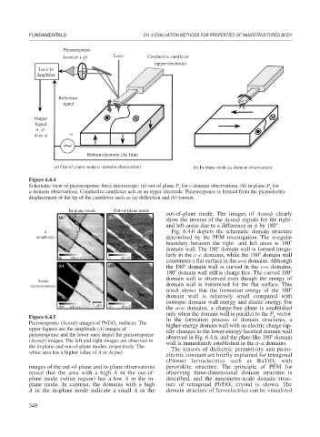
Piezoresponse
Acos( t + ) Laser Conductive cantilever
(upper electrode)
Lock-in
Amplifier
Reference
signal
Output
Signal
A,
Acos
Bottom electrode (Au film)
(a) Out-of-plane mode (c-domain observation) (b) In-plane mode (a-domain observation)
Figure 6.4.4
Schematic view of piezoresponse force microscope: (a) out-of-plane P for c-domain observations, (b) in-plane P for
s
s
a-domain observations. Conductive cantilever acts as an upper electrode. Piezoresponse is formed from the piezoelectric
displacement of the tip of the cantilever such as (a) deflection and (b) torsion.
In-plane mode Out-of-plane mode
out-of-plane mode. The images of Acos clearly
show the inverse of the Acos signals for the right-
and left-areas due to a difference in by 180 .
A Fig. 6.4.6 depicts the schematic domain structure
(amplitude) determined by the PFM investigation. The irregular
boundary between the right- and left areas is 180
domain wall. The 180 domain wall is formed irregu-
larly in the c–c domains, while the 180 domain wall
40 400 mV -3 50 mV
constitutes a flat surface in the a–a domains. Although
the 180 domain wall is curved in the c–c domains,
180 domain wall still is charge free. The curved 180
domain wall is observed even though the energy of
Acos
(piezoresponse) domain wall is minimized for the flat surface. This
result shows that the formation energy of the 180
domain wall is relatively small compared with
isotropic domain wall energy and elastic energy. For
2 m
-400 400 mV -40 60 mV the a–a domains, a charge-free plane is established
only when the domain wall is parallel to the P vector.
s
Figure 6.4.5 In the formation process of domain structures, a
Piezoresponse (Acos ) images of PbTiO surfaces. The
3 higher-energy domain wall with an electric charge rap-
upper figures are the amplitude (A) images of idly changes to the lower-energy facetted domain wall
piezoresponse and the lower ones depict the piezoresponse observed in Fig. 6.4.6, and the plate-like 180 domain
(Acos ) images. The left and right images are observed in wall is immediately established in the a–a domains.
the in-plane and out-of-plane modes, respectively. The The tensors of dielectric permittivity and piezo-
white area has a higher value of A or Acos .
electric constant are briefly explained for tetragonal
(P4mm) ferroelectrics such as BaTiO 3 with
images of the out-of-plane and in-plane observations perovskite structure. The principle of PFM for
reveal that the area with a high A in the out-of- observing three-dimensional domain structure is
plane mode (white region) has a low A in the in- described, and the nanometer-scale domain struc-
plane mode. In contrast, the domains with a high ture of tetragonal PbTiO crystal is shown. The
3
A in the in-plane mode indicate a small A in the domain structure of ferroelectrics can be visualized
348