
Page 375 - Book Hosokawa Nanoparticle Technology Handbook
P. 375
6.4 ELECTRIC PROPERTIES FUNDAMENTALS
[10] T. Tsurumi, S. Wada: Ceramics, 40, 354–368 (2005),
180° domain wall
in Japanese.
[11] Y. Saito, H. Takao, T. Tani, T. Nonoyama, K. Takatori,
90° domain wall
T. Homma, T. Nagaya and M. Nakamura: Nature, 432,
84–86 (2004).
[12] Y.P. Guo, K. Kakimoto and H. Ohsato: Appl. Phys.
Lett., 85, 4121–4123 (2004).
[13] Landolt-Bornstein, Vol. 11, New Series Group 3,
Springer-Verlag Heidelberg, New York (1979).
[14] H. Okino, T. Ida, H. Ebihara, H. Yamada, K. Matsushige
and T. Yamamoto: Jpn. J. Appl. Phys., 40, 5828–5832
(2001).
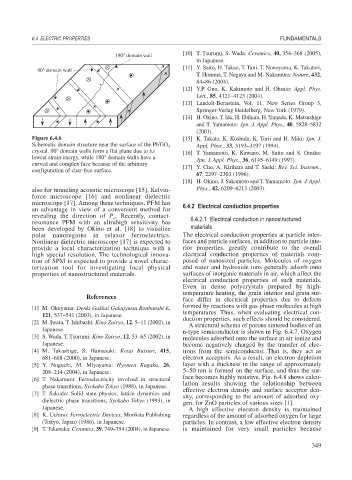
Figure 6.4.6 [15] K. Takata, K. Kushida, K. Torii and H. Miki: Jpn. J.
Schematic domain structure near the surface of the PbTiO Appl. Phys., 33, 3193–3197 (1994).
3
crystal. 90 domain walls form a flat plane due to its [16] T. Yamamoto, K. Kawano, M. Saito and S. Omika:
lowest strain energy, while 180 domain walls have a Jpn. J. Appl. Phys., 36, 6145–6149 (1997).
curved and complex face because of the arbitrary [17] Y. Cho, A. Kirihara and T. Saeki: Rev. Sci. Instrum.,
configuration of char-free surface.
67, 2297–2303 (1996).
[18] H. Okino, J. Sakamoto and T. Yamamoto: Jpn. J. Appl.
also for tunneling acoustic microscope [15], Kelvin- Phys., 42, 6209–6213 (2003).
force microscope [16] and nonlinear dielectric
microscope [17]. Among these techniques, PFM has 6.4.2 Electrical conduction properties
an advantage in view of a convenient method for
revealing the direction of P . Recently, contact- 6.4.2.1 Electrical conduction in nanostructured
s
resonance PFM with an ultrahigh sensitivity has
been developed by Okino et al. [18] to visualize materials
polar nanoregions in relaxor ferroelectrics. The electrical conduction properties at particle inter-
Nonlinear dielectric microscope [17] is expected to faces and particle surfaces, in addition to particle inte-
provide a local characterization technique with a rior properties, greatly contribute to the overall
high special resolution. The technological innova- electrical conduction properties of materials com-
tion of SPM is expected to provide a novel charac- posed of nanosized particles. Molecules of oxygen
terization tool for investigating local physical and water and hydroxide ions generally adsorb onto
properties of nanostructured materials. surfaces of inorganic materials in air, which affect the
electrical conduction properties of such materials.
Even in dense polycrystals prepared by high-
temperature heating, the grain interior and grain sur-
References
face differ in electrical properties due to defects
formed by reactions with gas-phase molecules at high
[1] M. Okuyama: Denki Gakkai Gakujyutsu Ronbunshi E,
temperatures. Thus, when evaluating electrical con-
121, 537–541 (2003), in Japanese.
duction properties, such effects should be considered.
[2] M. Iwata, T. Ishibashi: Kino Zairyo, 12, 5–11 (2002), in
A structural schema of porous sintered bodies of an
Japanese.
n-type semiconductor is shown in Fig. 6.4.7. Oxygen
[3] S. Wada, T. Tsurumi: Kino Zairyo, 12, 53–65 (2002), in molecules adsorbed onto the surface in air ionize and
Japanese. become negatively charged by the transfer of elec-
[4] M. Takashige, S. Hamasaki: Kotai Butsuri, 415, trons from the semiconductor. That is, they act as
681–688 (2000), in Japanese. electron acceptors. As a result, an electron depletion
[5] Y. Noguchi, M. Miyayama: Hyomen Kagaku, 26, layer with a thickness in the range of approximately
208–214 (2004), in Japanese. 5–50 nm is formed on the surface, and thus the sur-
face becomes highly resistive. Fig. 6.4.8 shows calcu-
[6] T. Nakamura: Ferroelectricity involved in structural
lation results showing the relationship between
phase transitions, Syokabo Tokyo (1988), in Japanese.
effective electron density and surface acceptor den-
[7] T. Sakudo: Solid state physics; lattice dynamics and
sity, corresponding to the amount of adsorbed oxy-
dielectric phase transitions, Syokabo Tokyo (1993), in
gen, for ZnO particles of various sizes [1].
Japanese. A high effective electron density is maintained
[8] K. Uchino: Ferroelectric Devices, Morikita Publishing regardless of the amount of adsorbed oxygen for large
(Tokyo, Japan) (1986), in Japanese. particles. In contrast, a low effective electron density
[9] T. Takenaka: Ceramics, 39, 749–754 (2004), in Japanese. is maintained for very small particles because
349