
Page 461 - Book Hosokawa Nanoparticle Technology Handbook
P. 461
4 MICROELECTRONICS PACKAGING BY METAL NANOPARTICLE PASTES APPLICATIONS
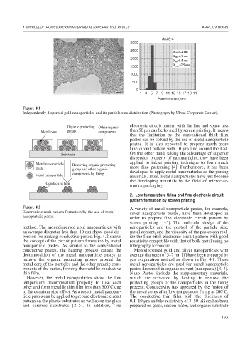
Au#8-4
3000
2500 D 10 =4.2 nm
D 50 =4.9 nm
2000
D 90 =5.5 nm
D max =7.5 nm
1500
1000
500
0
1 3 5 7 9 111315171911
Particle size (nm)
Figure 4.1
Independently dispersed gold nanoparticles and its particle size distribution (Photograph by Ulvac Corporate Center).
electronic circuit pattern with the line and space less
Organic protecting Other organic
Metal core group components than 50 m can be formed by screen printing. It means
that the limitation by the conventional thick film
pastes can be solved by the use of metal nanoparticle
pastes. It is also expected to prepare much more
fine circuit pattern with 10 m line around the LSI.
Substrate On the other hand, taking the advantage of superior
dispersion property of nanoparticles, they have been
applied to inkjet printing technique to form much
Metal nanoparticle Removing organic protecting
paste group and other organic more fine patterning [4]. Furthermore, it has been
components by firing developed to apply metal nanoparticles as the joining
Metal nanoparticle
materials. Thus, metal nanoparticles have just become
the developing materials in the field of microelec-
Conductive film
tronics packaging.
2. Low temperature firing and fine electronic circuit
pattern formation by screen printing
Figure 4.2 A variety of metal nanoparticle pastes, for example,
Electronic circuit pattern formation by the use of metal silver nanoparticle pastes, have been developed in
nanoparticle paste. order to prepare fine electronic circuit pattern by
screen printing [1–5]. The molecular design of the
method. The monodispersed gold nanoparticles with nanoparticles and the control of the particle size,
an average diameter less than 10 nm show good dis- metal content, and the viscosity of the pastes can real-
persion for making conductive pastes. Fig. 4.2 shows ize the fine pitch electronic circuit pattern with good
the concept of the circuit pattern formation by metal resistivity compatible with that of bulk metal using no
nanoparticle pastes. As similar to the conventional lithography technique.
conductive pastes, the heating process causes the Monodispersed gold and silver nanoparticles with
decomposition of the metal nanoparticle pastes to average diameter of 3–7 nm [1] have been prepared by
remove the organic protecting groups around the gas evaporation method as shown in Fig. 4.1. These
metal core of the particles and the other organic com- metal nanoparticles are used for metal nanoparticle
ponents of the pastes, forming the metallic conductive pastes dispersed in organic solvent (nanopaste) [3, 4].
thin film. Nano Pastes include the supplementary materials,
However, the metal nanoparticles show the low which are activated by heating to remove the
temperature decomposition property to fuse each protecting groups of the nanoparticles in the firing
other and form metallic thin film less than 300 C due process. Conductivity has appeared by the fusion of
to the quantum size effect. As a result, metal nanopar- the metal cores after low temperature firing at 200 C.
ticle pastes can be applied to prepare electronic circuit The conductive thin film with the thickness of
pattern on the plastic substrates as well as on the glass 0.1–10 m and the resistivity of 3–50 cm has been
and ceramic substrates [2–5]. In addition, fine prepared on glass, silicon wafer, and organic substrate
435