Page 458 - Book Hosokawa Nanoparticle Technology Handbook
P. 458

APPLICATIONS                                 3 SENSING BASED ON LOCALIZED SURFACE PLASMON RESONANCE
                            APPLICATION 3

                    3       SENSING BASED ON LOCALIZED SURFACE PLASMON RESONANCE IN METALLIC
                            NANOPARTICLES


                  1. Localized surface plasmon                   where  r stands for radius of the nanosphere.  The
                                                                 polarizability   ( ) is maximum with the minimum
                  Gold nanospheres dispersed in a solution are ruby red,  absolute value of the denominator. When the nanos-
                  since green light interacts with electrons in the nanos-  phere is covered with a dielectric thin film with a
                  pheres and is adsorbed. This phenomenon is called  thickness  d and dielectric constant    ( ), equation
                                                                                                d
                  localized surface plasmon resonance (LPR). Localized  (3.1) is rewritten as
                  surface plasmon resonance occurs not only in metallic
                  nanoparticles but also in a sharp metallic tip and at a                 ()      () ()

                                                                                     ()
                                                                                              m
                                                                                                  B

                  rough metallic surface.  These LPR phenomena are     ()   4    ()(r    ) d  3  d  A    () (()   (3.2)
                                                                         m

                                                                                     ()
                  applied to enhancement of near-field scanning                           ()   2  m  B
                                                                                       A
                                                                                    d
                  microscopy, Raman scattering and fluorescence spec-
                  troscopy. LPR has the following features:      where the parameters are described as
                    (1) Confinement of light within a nanometer region.
                                                                            ()       ()(3   2P )   2    ()P  (3.3)
                    (2) The sensitive resonance condition to the dielec-   A     a            d
                       tric constant of the ambient medium.
                                                                            ()       ()      ()(3   P )  (3.4)
                                                                                    P
                                                                                        d
                                                                                 a
                                                                           B
                    (3) A large electric field produced at the LPR
                       condition.                                                  ⎛  r  ⎞ 3
                                                                             P   1   ⎜  ⎟               (3.5)
                                                                                       d
                  Recently, nano- and micro-photonic devices and sen-              ⎝  r   ⎠
                  sors have been developed, based on LPR. This article
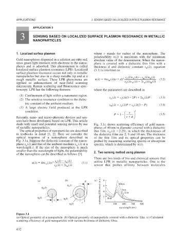
                  deals with small and potential sensing devices by use  Fig. 3.1c shows scattering efficiency of gold nanos-
                  of metallic nanoparticles.                     pheres of 40 nm in diameter covered with a dielectric
                    The optical properties of nanoparticles are described  thin film (  ( )  2.25), in which the thicknesses of
                                                                          d
                  in textbooks in detail [1, 2]. Here we consider the  the dielectric film are 2, 5 and 10 nm. The thickness
                  optical response of a nanosphere described in  of the thin film and its optical properties can be
                  Fig. 3.1a. Suppose the dielectric constant of the nanos-  probed by measuring scattering spectra or absorption
                  phere   ( ) and that of the ambient medium   ( ) at a  spectra, which is determined by  ( ).
                                                      m
                        a
                  wavelength  . If the size of the nanosphere is much
                  smaller than the wavelength of light, the polarizability  2. Two sensing method using plasmon
                  of the nanosphere can be described as follows [3].
                                                                 There are two kinds of bio and chemical sensors that

                                            ()     ()

                              ()   4    ()r  3  a  m     (3.1)   utilize LPR in metallic nanoparticles. One is the
                                   m

                                            ()    2   ()         sensor that probes affinity between molecules
                                         a
                                                m
                               (a)             (b)         d     (c)  8
                                                e m (l)               6        10nm
                                 e m (l)                            scattering Efficiency (a.u.)  4  5nm
                                                                                   2nm
                               e a (l)        e a (l)                 2  0nm
                                        r
                                                         r
                                                  e d (l)                   500  600   700  800
                                                                                wavelength (nm)
                  Figure 3.1
                  (a) Optical geometry of a nanoparticle. (b) Optical geometry of nanoparticle covered with a dielectric film. (c) Calculated
                  scattering efficiency of gold nanoparticles with various thickness of dielectric films.
                  432
   453   454   455   456   457   458   459   460   461   462   463