
Page 463 - Book Hosokawa Nanoparticle Technology Handbook
P. 463
4 MICROELECTRONICS PACKAGING BY METAL NANOPARTICLE PASTES APPLICATIONS
There may be a risk of electromigration of silver
in the case of electronic devices using silver con-
ductors. In order to solve the problem, a new type of
silver–palladium alloy nanoparticle paste with
desired Ag–Pd ratio (Fig. 4.4b) has been prepared
[5]. Silver–palladium alloy nanoparticle paste with
Ag85–Pd15 ratio affords the conductive film of the
thickness of 4 m and the resistivity of 12 cm,
showing the anti-electromigration property.
Monodispersed silver nanoparticles prepared by
gas evaporation method are used for a hybrid type
silver paste, where silver nanoparticles are mixed
with micron size silver powder (average diameter
3–5 m) [1, 6]. After firing the hybrid silver paste,
the small size of silver particles are filled in the
vacancy between the large silver particles to form
tight conductive film to reinforce the electric contact
and reduce the resistivity. Such hybrid paste shows a
good performance to form a reliable fired film com-
pared to the conventional silver paste.
Silver nanoparticle pastes with high viscosity and
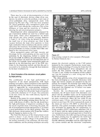
thixotropy for the screen printing are also used for the Figure 4.5
patterning by the dispensing method to realize the Inkjet printing example by silver nanopaste (Photograph
18 m line width. In addition, the patterning by the dis- by Harima Chemicals, Inc.).
pensing technique can repair the disconnection part of
the circuit. For example, metal nanoparticle pastes are
injected on the disconnection part of the PDP elec- prepare the electronic patterns as the CAD pattern
trodes by the dispensing method, and then the part is prepared by the computer. Furthermore, recent super-
recovered to be conductive through the heat treatment inkjet printing technology [7] using the femto liter (fl)
by the laser irradiation [3]. drop of monodispersed silver nanoparticle ink can
realize the fine patterns with the line and space
3.6 m/1.4 m. Further development of this technol-
3. Direct formation of the electronic circuit pattern ogy may be expected as a new wiring tool for the
by inkjet printing superfine packaging.
The inkjet printing using silver nanoparticle paste
The combination of the high performance of has been developing as a printable electronics tech-
dispersion of the metal nanoparticles with inkjet nique and various samples are prepared for the esti-
printing can realize a direct formation of the superfine mation. For example, the electrode (line width 50 m,
patterning with the line width of several micrometers, fired thickness 2 m, resistivity 2 cm) of the PDP
which is impossible by screen-printing technique. front panel (the diagonal size 10 inches) was manu-
In the case of inkjet printing, the minimum quantity of factured on trial [8].
liquid, 2 pl, coming from the printer head corresponds Besides the two-dimensional circuit pattern
to a dot with a diameter of 15–16 m. The connection formation, the 20 layers board with alternative con-
of the dots forms the line width directly figured by ductor and the insulator layers can be manufactured
inkjet printing. by the use of silver nanoparticle paste and the insula-
Instead of the pastes for screen printing, the metal tor paste, respectively, where the line width 50 m,
nanoparticle ink for inkjet printing shows the low vis- minimum space 110 m, and thickness 4 m are pat-
cosity with dozens of mPa·s, thus the ink should have terned on each layer [9]. Silver nanoparticle pastes in
the high performance of dispersion avoiding to clog the sheets are fired at 150–200 C to afford the con-
the nozzle of printer head. Concerning this point, the ductivity. Fine pattern formation technique has been
ink of monodispersed metal nanoparticles [3, 4] shows also developed for making the low temperature co-
a good performance for the inkjet printing. Thus, the firing ceramics (LTCC) multi-layer substrates [10]. A
fine electronic circuit pattern with 20 m line width is set of sheets with the inkjet printed pattern using sil-
directly figured as shown in Fig. 4.5. ver nanoparticle paste are packaged and co-fired all at
The fired film thickness of the inkjet printed circuit once. Furthermore, the multi-layering technique using
pattern is about 1–2 m, but the control of the paste the inkjet printing may be applied to the multi-layer
viscosity and the ejection voltage of the printer head, substrates embedded with IC and capacitors, the
the surface treatment of the substrates, the heat treat- flexible substrates embedded with the super high den-
ment conditions, and the printing technique can easily sity system module and the electronic components,
437