
Page 462 - Book Hosokawa Nanoparticle Technology Handbook
P. 462
APPLICATIONS 4 MICROELECTRONICS PACKAGING BY METAL NANOPARTICLE PASTES
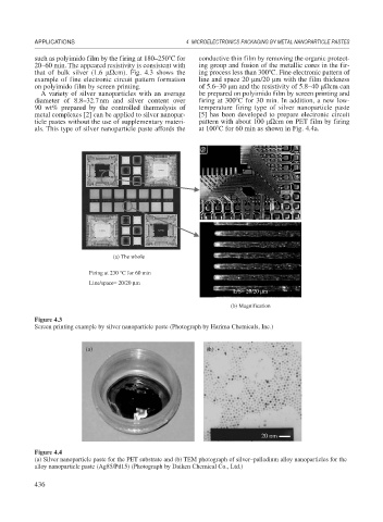
such as polyimido film by the firing at 180–250 C for conductive thin film by removing the organic protect-
20–60 min. The appeared resistivity is consistent with ing group and fusion of the metallic cores in the fir-
that of bulk silver (1.6 cm). Fig. 4.3 shows the ing process less than 300 C. Fine electronic pattern of
example of fine electronic circuit pattern formation line and space 20 m/20 m with the film thickness
on polyimido film by screen printing. of 5.6–30 m and the resistivity of 5.8–40 cm can
A variety of silver nanoparticles with an average be prepared on polyimido film by screen printing and
diameter of 8.8–32.7nm and silver content over firing at 300 C for 30 min. In addition, a new low-
90 wt% prepared by the controlled thermolysis of temperature firing type of silver nanoparticle paste
metal complexes [2] can be applied to silver nanopar- [5] has been developed to prepare electronic circuit
ticle pastes without the use of supplementary materi- pattern with about 100 cm on PET film by firing
als. This type of silver nanoparticle paste affords the at 100 C for 60 min as shown in Fig. 4.4a.
(a) The whole
Firing at 230 °C for 60 min
Line/space= 20/20 μm
L/S= 20/20 μm
(b) Magnification
Figure 4.3
Screen printing example by silver nanoparticle paste (Photograph by Harima Chemicals, Inc.)
(a) (b)
20 nm
Figure 4.4
(a) Silver nanoparticle paste for the PET substrate and (b) TEM photograph of silver–palladium alloy nanoparticles for the
alloy nanoparticle paste (Ag85/Pd15) (Photograph by Daiken Chemical Co., Ltd.)
436