
Page 367 - Op Amps Design, Applications, and Troubleshooting
P. 367
344 DIGITAL-TO-ANALOG AND ANALOG-TO-DIGITAL CONVERSION
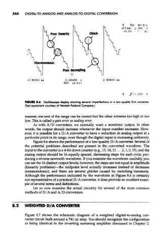
FIGURE 8.6 Oscilloscope display showing several imperfections in a low-quality D/A converter.
(Test equipment courtesy of Hewlett-Packard Company.)
manner, one end of the range can be correct but the other extreme too high or too
low. This is called a gain error or scaling error.
As with A/D converters, we normally want a monotonic output. In other
words, the output should increase whenever the input number increases. How-
ever, it is possible for a D/A converter to have a reduction in analog output at a
particular point in its range, even though the digital input is increasing uniformly.
Figure 8.6 shows the performance of a low-quality D/A converter. Several of
the potential problems described are present in the converted waveform. The
input to the converter is a 4-bit down counter (e.g., 15,14,13... 2,1,0,15), and the
analog output should be 16 equally spaced, decreasing steps for each cycle, pro-
ducing a reverse sawtooth waveform. If you examine the waveform carefully, you
can see the 16 distinct output levels; however, the steps are not equal in amplitude
(linearity problems)—the midpoint level actually increases instead of decreases
(nonmonotonic), and there are several glitches caused by switching transients.
Although the performance indicated by the waveform in Figure 8.6 is certainly
not representative of a practical D/A converter, it does provide an excellent exam-
ple of several terms and definitions.
Let us now examine the actual circuitry for several of the more common
methods of D/A and A/D conversion.
8.2 WEIGHTED D/A CONVERTER
Figure 8.7 shows the schematic diagram of a weighted digital-to-analog con-
verter circuit built around a 741 op amp. You should recognize the configuration
as being identical to the inverting summing amplifier discussed in Chapter 2.