
Page 372 - Op Amps Design, Applications, and Troubleshooting
P. 372
Parallel A/D Converter 349
trates the principles involved and would be adequate for many D/A applications.
The linearity could be greatly improved by using precision resistors (rather than 5
percent) and by driving the digital inputs via analog switches (rather than directly
from the output of a digital counter). Figure 8.9(a) shows the actual output of the
converter, with the 16 distinct output levels in the waveform easily seen. Figure
8.9(b) shows the same basic circuit after the output has gone through a simple
low-pass filter. The abrupt changes in the output are now gone, leaving us with a
cleaner analog signal.
For noncritical applications, construction of your own D/A converters is fea-
sible. However, the low cost and high performance (e.g., laser-trimmed ladder
resistors) available in integrated converters makes these devices the best choice
for many applications. An example of such a device is the TDC1016 10-bit D/A
converter manufactured by Raytheon Semiconductor.
8.4 PARALLEL A/D CONVERTER
Parallel A/D conversion (sometimes called flash conversion) is the fastest tech-
nique available and the simplest to understand. However, its practicality is lim-
N
ited to small numbers of bits, since it requires 2 -1 comparator circuits in order to
produce an N-bit digital output. For example, producing a 3-bit digital output (8
3
states) requires 2 - 1, or 7, comparator circuits plus a significant amount of logic
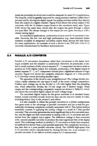
circuitry. Figure 8.10 shows the complete schematic diagram of a 3-bit parallel
A/D converter circuit (including decoder logic).
The operation of the circuit is very straightforward. The voltage divider pro-
vides a stable reference for one input of each of the seven voltage comparators.
Further, each voltage tap on the divider is 1.25 volts higher than the preceding
one, which effectively divides the 10-volt range into 8 distinct ranges. These
ranges and the corresponding comparator outputs are shown in Table 8.3, which
also shows the converted digital output for each voltage range.
The converted digital output for the given converter is in standard binary
format. Actual converter circuits, however, may use any one of a variety of codes,
including binary, Gray Code, excess-3, and others.
It is also possible to utilize the parallel converter in a hybrid configuration
that gains some of the advantage of parallel conversion and yet avoids the geo-
metrically increasing complexity normally associated with it. This hybrid method
essentially consists of applying the analog voltage to a small (4-7 bits) parallel
converter. This converter generates the most significant bits in the converted num-
ber, and the digits are then reconverted to analog with a D/A converter and sub-
tracted from the original input signal. The difference voltage is then converted
with a second parallel converter to produce the least significant bits of the digital
result. This multistage method of parallel A/D conversion is faster than nonparal-
lel methods but slower than a pure parallel approach. The complexity, however, is
less than that of a pure parallel converter circuit. The AD9028 high-speed 8-bit
A/D converter circuit, manufactured by Analog Devices, Inc., is an example of a
parallel converter. It can deliver an 8-bit output in 3.3 nanoseconds.