
Page 377 - Op Amps Design, Applications, and Troubleshooting
P. 377
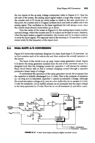
Dual-Slope A/D Conversion  353


               the two inputs of the op amp voltage comparator (refer to Figure 8.11). Near the
               left side of the screen, the analog input signal makes a large step change. It takes
               the counter and A/D circuit six clock pulses to climb to the new input level At
               this point, the counter and A/D signal oscillate back and forth on either side of the
               analog signal. This oscillation in the least significant bit will always occur, since
               the counter must always count either up or down.
                    Near the center of the screen in Figure 8.12, the analog input makes another
               upward change, which the counter and D/A output can be seen to track. Similarly,
               when the input makes a negative transition, the counter and D/A output continue
               to track the input signal. The response time of the tracking A/D converter is deter-
               mined solely by the frequency of the input clock.


        8.6    DUAL-SLOP! A/D CONVERSION

               Figure 8.13 shows the schematic diagram of a basic dual-slope A/D converter. Let
               us first examine each of its subcircuits and then analyze the overall operation of
               the circuit.
                    The heart of the circuit is an op amp, linear ramp generator circuit. Figure
               8.14 shows the ramp generator isolated from the rest of the converter circuit. It is
               designed such that the charging current for capacitor C will always be constant.
               Basic circuit theory tells us that a constant charging current through a capacitor
               produces a linear ramp of voltage.
                    To understand the operation of the ramp generator circuit, let us assume that
               the capacitor is initially discharged (i.e., 0 volts). This is the purpose of transistor
               Qi—as long as it is saturated, capacitor C cannot accumulate a charge. Although
               the actual saturation voltage of Qi may be a few millivolts, let us assume it is truly
               0 volts for simplicity. Let us further assume (as an example) that the input voltage
               to the ramp generator is +5 volts. Now let us cut off transistor Qi and allow capac-


                          FIGURE 8.13 A basic dual-slope analog-to-digital converter circuit.