
Page 444 - Organic Electronics in Sensors and Biotechnology
P. 444
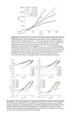
–25.0       5 μm (1)
                                     2 μm (2)
                                                    4
                         –20.0       1 μm (3)               3
                                    500 nm (4)
                                    270 nm (5)             2
                         –15.0
                        I ds (μA)               5
                         –10.0
                                                           1
                          –5.0

                          0.0
                       290 K  0       –10     –20      –30     –40
                       V g  = –40 V
                                             V ds  (V)
               FIGURE 1.6  Drain current as a function of source-to-drain voltage for different
               channel lengths. The characterization was taken at room temperature and
               high density of charge carriers (V =−40 V, well beyond threshold voltages of
                                       g
               each channel). For observation of the scaling behavior, the W/L ratios of all
               channels were kept at the same value of 10 in fabrication to exclude
               geometric factors. Clearly in the regime of V  < V − V , the current-voltage
                                                ds  g  th
               characteristic transitions from linear to superlinear upon scaling from micron
               to submicron channel length. For submicron channels there is an exponential
               dependence at very small V  due to the injection-limited transport through
                                    ds
               Schottky barrier at the metal-semiconductor contact. (Reprinted with
               permission from Ref. 60. Copyright 2007, American Institute of Physics.)
               10 –1                        10 –1
               10 –2                        10 –2
               10 –3                        10 –3
                  Ohmic                     10 –4
               10 –4
              I ds /W (A/cm)  10 –5   5 μm  I ds /W (A/cm)  10 –5  Ohmic  5 μm
                                                                   2 μm
                                      2 μm
                                      1 μm
                                                                   1 μm
               10 –6
                                      500 nm  10 –6               500 nm
                                      270 nm                      270 nm
               10 –7                  180 nm  10 –7               180 nm
                                      130 nm                      130 nm
               10 –8                  100 nm  10 –8               100 nm
                                      80 nm                        80 nm
               290 K  10 4   10 5     10 6  125 K  10 4   10 5    10 6
               V g  = –40 V                 V g  = –40 V
                          V ds /L (V/cm)               V ds /L (V/cm)
               10 –1                        10 –1
                     5 μm                         5 μm
                     2 μm                         2 μm
               10 –2  1 μm                  10 –2  1 μm
                    500 nm                       500 nm
               10 –3  270 nm                10 –3  270 nm
                    180 nm                  10 –4  180 nm
                                                 130 nm
                    130 nm
              I ds /W (A/cm)  10 –5  100 nm  I ds /W (A/cm)  10 –5  100 nm
               10 –4
                    80 nm
                                                 80 nm
                                            10 –6
               10 –6
               10 –7  Ohmic                 10 –7  Ohmic
               10 –8                        10 –8
               57 K  10 4    10 5     10 6  4.8 K  10 4   10 5    10 6
               V g  = –40 V                 V g  = –40 V
                          V ds /L (V/cm)               V ds /L (V/cm)
          FIGURE 1.8  The current density vs. longitudinal fi eld plots for various channel lengths
          at four different temperatures. The solid lines in these plots are the ohmic channel
          transport currents, calculated based on the mobility extracted from long-channel (5 μm)
          devices. These lines serve as the references to investigate the issues of contact
          injection-limited transport and fi eld-dependent mobility. All the four fi gures are exactly
          on the same scale for the purpose of comparison.