
Page 445 - Organic Electronics in Sensors and Biotechnology
P. 445
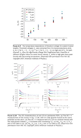
0
                              270 nm
                       –2
                              500 nm
                       –4
                                1 μm
                       –6
                                2 μm
                       –8
                                5 μm
                      –10
                     V th  (V)  –12
                      –14
                      –16
                      –18
                      –20
                      –22
                            50     100    150    200   250    300
                                            T (K)
               FIGURE 1.9  The temperature dependence of threshold voltage for scaled channel
               lengths. Threshold voltages V  were extracted from the transconductance plots
                                    th
                                   1/2
               (I  vs. V  for V  < V  – V ; (I )  vs. V  for V ≥ V  – V ) on high end of V  for each
                d    g   ds  g  th  d    g   ds  g  th          ds
               channel. V  does not signifi cantly change with longitudinal fi eld. Channels of
                       th
               different lengths follow the same trend; namely, V  shifts to high gate bias quasi-
                                                  th
               linearly with decreasing temperature. (Reprinted with permission from Ref. 60.
               Copyright 2007, American Institute of Physics.)
                –600.0n
                                            –250.0n
                      V g  =                      V g  =
                –500.0n  0 V                        0 V
                       –6 V                 –200.0n  –6 V
                –400.0n  –12 V                     –12 V
                      –18 V                 –150.0n  –18 V
                      –24 V
                                                   –24 V
               I ds  (A)  –300.0n  –30 V   I ds  (A)  –100.0n  –30 V
                –200.0n
                                            –50.0n
                –100.0n
                                              0.0
                  0.0
                     0            –1           –2            –3           –4            –5  0            –1            –2           –3   –4           –5
                             V ds  (V)                   V ds  (V)
                              (a)                         (b)
                 –16.0                       –17.0
                 –16.5
                                             –17.5
                 –17.0
                                             –18.0
                 –17.5                       –18.5
                ln (I ds /V ds )  –18.0     ln (I ds /V ds )  –19.0
                 –18.5
                 –19.0
                 –19.5                       –19.5
                                             –20.0
                 –20.0
                                             –20.5
                 –20.5
                                             –21.0
                     0             1             2             3             4             5  0             1             2             3             4             5
                           |1/V ds | (V –1 )           |1/V ds | (V –1 )
                              (c)                        (d)
          FIGURE 1.14  The DC characteristics of sub-10-nm pentacene FETs. (a) The DC I–V
          measurement of the device in Fig. 1.13b, with the side guards biased at the same
          potential as the drain. (b) The DC I–V measurement of a 19 nm channel device with
          the side guards biased; I /I increases with increasing |V |. (c) ln(I /V ) vs. 1/|V |
                             ds                     g      ds  ds     ds
          plot of the data in (a). (d) ln(I /V ) vs. 1/|V | plot of the data in (b). (Reprinted with
                                ds  ds    ds
          permission from Ref. 40. Copyright 2004, American Institute of Physics.)