
Page 446 - Organic Electronics in Sensors and Biotechnology
P. 446
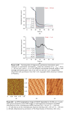
1.2
                                                    Grain ~ 140 nm
                            1.0
                           Normalized drain current  0.8  2 μm


                            0.6
                                     4 μm
                            0.4
                                     6 μm
                            0.2     12 μm
                                    36 μm
                            0.0
                                0    10  20   30   40   50   60
                                            Time (s)
                                              (a)
                             1.2
                                                     Grain ~ 1 μm
                           Normalized drain current  0.8  2 μm
                             1.0


                             0.6
                                      4 μm
                             0.4
                                      6 μm
                             0.2     12 μm
                                     36 μm
                             0.0
                                0    10  20   30   40   50   60
                                            Time (s)
                                              (b)
               FIGURE 1.20   Sensing data of large-scale pentacene transistors upon
               exposure to 1-pentanol: normalized I  under the condition of V = V = –25 V,
                                           ds                 g  ds
               v = 45 mL/min, and d = 2 mm for different microscale channel lengths, with
               average pentacene grain size of (a) 140 nm and (b) 1 μm, respectively.
               (Reprinted with permission from Ref. 115. Copyright 2004, American Institute
               of Physics.)

                              1.00

                              0.75

                              0.50

                              0.25

                              0
           0  0.25  0.50  0.75  1.00
                    (a)                   (b)                  (c)
          FIGURE 2.6  (a) AFM topographical image of D3ANT deposited on Si/SiO  (1 × 1 μm)
                                                               2
          and typical constant-current STM images of self-organized monolayers of D3ANT
                                                         2
          adsorbed (b) at the n-tetradecane–HOPG interface (16 × 16 nm ; V =−333 mV;
                                                           t
                                                              2
          I = 27 pA) and (c) at the n-tetradecane–Au(111) interface (16 × 16 nm ; V =−62 mV;
           t                                                    t
          I = 83 pA). (Reproduced by permission of The Royal Society of Chemistry, Ref. 131.)
           t