
Page 285 - Phase-Locked Loops Design, Simulation, and Applications
P. 285
MIXED-SIGNAL PLL APPLICATIONS PART 2: FRACTIONAL-N FREQUENCY
SYNTHESIZERS Ronald E. Best 169
are marked by dots. When observing U during an extended period of time, note that U is 1
Q
Q
in 70 percent of all samples, and 0 in the remaining 30 percent. The quantization error
sequence e is plotted in Fig. 7.6c. e(nT ) is now a random sequence with mean 0. To get rid of
the ripple in the output signal of the quantizer, a digital lowpass filter is used as the
postprocessing block G (Fig. 7.5d). This filter is used to decimate the output signal of the
quantizer—thus, the output of the filter is read out at a lower sampling rate f . To avoid
S
aliasing, the filter must remove all frequencies above f /2—in other words, the cutoff
S
frequency filter must be f /2 or less. The ratio f /f is called the oversampling ratio (OSR).
S F S
What is the impact of that lowpass filter onto the quantized signal? To answer this question we
must consider the power spectral density (PDS) of the error sequence e(nT ). Because e is
purely random, the PDS of the error sequence is flat in the range −f /2 to f /2, as shown in
F F
Fig. 7.6d. The PSD of the error sequence is denoted as S . Due to lowpass filtering, all
ee
spectral components of S above f /2 (and below −f /2) are removed. The PSD of the filtered
ee S S
error sequence is shown in Fig. 7.6e and is denoted as S . Total quantization error power is
yy
reduced by a factor OSR. Consequently, the amplitude (peak value) of the lowpass filtered
error sequence is reduced by the factor . Because we express the resolution of an ADC
in numbers of bits, the so-called bit gain G is given by
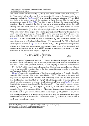
(7.3)
where ld signifies logarithm to the base 2. To make a numerical example, the bit gain G
becomes 3 for an oversampling ratio of 64—thus, the resulting ADC now has a resolution of
four bits. To obtain a bit gain of 15, however, the over-sampling ratio must be chosen as OSR
30
= 2 = 1,073,741,824, which is quite a large number! Obviously, there must be more efficient
ways to increase ADC resolution. Let’s therefore proceed to more powerful oversampling
configurations: the ΣΔ A/D converter.
Figure 7.7a shows the block diagram of the simplest configuration—a first-order ΣΔ ADC.
A one-bit ADC is preceded by an integrator (labeled “INT”). The quantized output signal
U which is a logical signal is converted back into analog format, and that analog signal is
Q
then fed back to a summing block on the left side of the schematic. It is assumed that all
signals are in the same range as in the previously discussed A/D converter (Fig. 7.5d). In order
to get a finite integrator output signal U , the difference U − U DAC must be zero on average.
i
A
Given U , the mean of U must equal U . When U is a DC level with value 0.5, for
A DAC A A
example, U DAC will be a sequence 101010 … The digital filter processing the output signal of
the one-bit ADC is again a lowpass filter, whose corner frequency is f /(2 OSR) or less, where
F
the oversampling ratio OSR is usally much greater than 1. To a first approximation, the output
D of the digital filter is the average of the quantized signal U (0.5 in this example) with a
Q
small superimposed ripple signal.
Printed from Digital Engineering Library @ McGraw-Hill (www.Digitalengineeringlibrary.com).
Copyright ©2004 The McGraw-Hill Companies. All rights reserved.
Any use is subject to the Terms of Use as given at the website.