
Page 108 - Photodetection and Measurement - Maximizing Performance in Optical Systems
P. 108
System Noise and Synchronous Detection
System Noise and Synchronous Detection 101
about 1 percent accuracy. For this reason, many applications avoid sinusoidal
demodulation, using instead the bipolar (square-wave) demodulation described
above. This is simpler to perform to high precision and high speed and is there-
fore much cheaper to integrate.
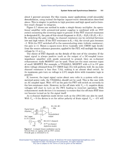
Figure 5.7 shows one method to make a simple binary multiplier. An opera-
tional amplifier with symmetrical power supplies is combined with an FET
switch connecting the inverting input to ground. If the FET channel resistance
is designated R 4, the gain of this circuit fragment is (R 1R 4 - R 2R 3)/(R 1(R 2 + R 4)).
By switching the gate voltage, its channel resistance can be switched between
low and high values. If the FET resistance is R 4 = 0W, the circuit gain becomes
-1. With the FET switched off to the nonconducting state (infinite resistance),
the gain is +1. Hence a square-wave drive (typically with CMOS logic levels)
from the source reference generator, applied to the FET, will multiply the input
voltage by ±1 at f mod.
The choice of FET depends on the details of the rest of the circuitry. If the
input signal is always positive (such as the output of a DC-coupled trans-
impedance amplifier with anode connected to ground, then an n-channel
enhancement mode MOSFET can be used. These are the most common types
of small MOSFET. For example, a VN2222LL MOSFET with a 0 to 5V gate
drive voltage obtained from 5V CMOS logic ICs will perform well. Its on-state
channel resistance is less than 7.5W, making it an almost ideal switch. As
its maximum gate turn on voltage is 2.5V, simple drive with transistor logic is
possible.
If, however, the input signal varies about zero volts in a system with sym-
metrical power rails, the VN2222LL should not be used. This is the case with
an AC coupled input. With +5V on the gate the FET will switch on correctly to
the low-resistance state. However, in the off state with V gs = 0, negative drain
voltages will start to turn on the FET, leading to incorrect operation. With
enhancement mode devices it is necessary to ensure that the off-state FET does
not become turned on by the signal itself.
An n-channel depletion-mode device such as the 2N4118A can also be used.
With V gs = 0 the device is on for either polarity of drain signal. V gs =-5V will
R1, R2, R3
R3
Signal input R1 = 10k
(bipolar) –
R2
+ Demodulated
Ref. input output
0–5V CMOS D
G R4 (FET channel)
S J177 (p-channel
10k depletion mode)
Figure 5.7 A simple binary modulator can be
formed from an opamp and an FET switch.
Overall gain is switched to ±1.
Downloaded from Digital Engineering Library @ McGraw-Hill (www.digitalengineeringlibrary.com)
Copyright © 2004 The McGraw-Hill Companies. All rights reserved.
Any use is subject to the Terms of Use as given at the website.