
Page 109 - Photodetection and Measurement - Maximizing Performance in Optical Systems
P. 109
System Noise and Synchronous Detection
102 Chapter Five
switch off the FET. As long as the signal is such that the drain voltage is more
positive than about -3V, the switching operation will be correct. Unfortunately,
most logic circuitry is traditionally arranged for positive signals.
A convenient practical configuration uses a p-channel depletion-mode
MOSFET such as a J177. As this is a “normally-on” device, in which channel
current flows when V gs = 0, the on state can handle bipolar signals. The off state
is obtained by putting V gs a few volts positive. It needs to be at least 2.25V more
positive than any voltage along the channel. This is convenient as the gate may
then be driven by 74HC or 4000 series CMOS logic to the positive rail (+5V or
up to +15V, respectively). The signal can then vary from the negative rail up to
within a couple of volts from the positive rail without difficulty. It is best to
drive this circuit from the low impedance output of an opamp.
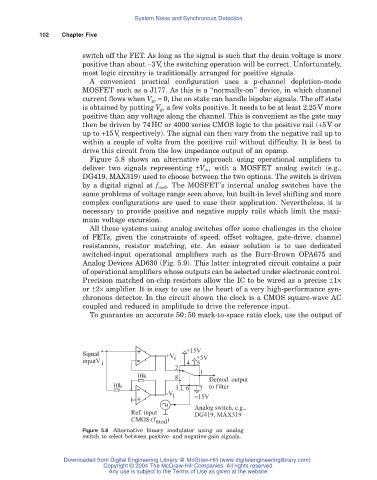
Figure 5.8 shows an alternative approach using operational amplifiers to
deliver two signals representing ±V in, with a MOSFET analog switch (e.g.,
DG419, MAX319) used to choose between the two options. The switch is driven
by a digital signal at f mod . The MOSFET’s internal analog switches have the
same problems of voltage range seen above, but built-in level shifting and more
complex configurations are used to ease their application. Nevertheless, it is
necessary to provide positive and negative supply rails which limit the maxi-
mum voltage excursion.
All these systems using analog switches offer some challenges in the choice
of FETs, given the constraints of speed, offset voltages, gate-drive, channel
resistances, resistor matching, etc. An easier solution is to use dedicated
switched-input operational amplifiers such as the Burr-Brown OPA675 and
Analog Devices AD630 (Fig. 5.9). This latter integrated circuit contains a pair
of operational amplifiers whose outputs can be selected under electronic control.
Precision matched on-chip resistors allow the IC to be wired as a precise ±1¥
or ±2¥ amplifier. It is easy to use as the heart of a very high-performance syn-
chronous detector. In the circuit shown the clock is a CMOS square-wave AC
coupled and reduced in amplitude to drive the reference input.
To guarantee an accurate 50:50 mark-to-space ratio clock, use the output of
+ +15V
Signal +V +5V
inputV i - i 4 5
2
1
10k 8 Demod. output
10k 3 6 7 to filter
-V i -15V
-
+
Analog switch, e.g.,
Ref. input DG419, MAX319
CMOS (f mod )
Figure 5.8 Alternative binary modulator using an analog
switch to select between positive- and negative-gain signals.
Downloaded from Digital Engineering Library @ McGraw-Hill (www.digitalengineeringlibrary.com)
Copyright © 2004 The McGraw-Hill Companies. All rights reserved.
Any use is subject to the Terms of Use as given at the website.