
Page 110 - Photodetection and Measurement - Maximizing Performance in Optical Systems
P. 110
System Noise and Synchronous Detection
System Noise and Synchronous Detection 103
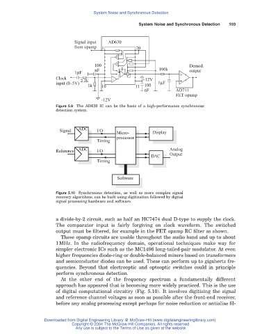
Signal input AD630
from opamp 1 20
A
100 B Demod.
nF 100k output
1μF +
Clock 2.2k + - +12V -
input (0–5V) 1μF
1k 10 11 100
nF AD711
FET opamp
-12V
Figure 5.9 The AD630 IC can be the basis of a high-performance synchronous
detection system.
Signal ADC I/O
Micro- Display
processor
Timing
ADC Analog
Reference I/O
DAC Output
Timing
Software
Figure 5.10 Synchronous detection, as well as more complex signal
recovery algorithms, can be built using digitization followed by digital
signal processing hardware and software.
a divide-by-2 circuit, such as half an HC7474 dual D-type to supply the clock.
The comparator input is fairly forgiving on clock waveform. The switched
output must be filtered, for example in the FET opamp RC filter as shown.
These opamp circuits are usable throughout the audio band and up to about
1MHz. In the radiofrequency domain, operational techniques make way for
simpler electronic ICs such as the MC1496 long-tailed-pair modulator. At even
higher frequencies diode-ring or double-balanced mixers based on transformers
and semiconductor diodes can be used. These can perform up to gigahertz fre-
quencies. Beyond that electrooptic and optooptic switches could in principle
perform synchronous detection.
At the other end of the frequency spectrum a fundamentally different
approach has appeared that is becoming more widely practiced. This is the use
of digital computational circuitry (Fig. 5.10). It involves digitizing the signal
and reference channel voltages as soon as possible after the front-end receiver,
before any analog processing except perhaps for noise reduction or antialias fil-
Downloaded from Digital Engineering Library @ McGraw-Hill (www.digitalengineeringlibrary.com)
Copyright © 2004 The McGraw-Hill Companies. All rights reserved.
Any use is subject to the Terms of Use as given at the website.