
Page 63 - Photodetection and Measurement - Maximizing Performance in Optical Systems
P. 63
Fundamental Noise Basics and Calculations
56 Chapter Three
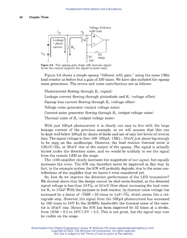
Voltage Follower
I p e n with Gain
Leakage i n
+ photo
current R L
V b R2
R1 99k0
1k0
Figure 3.6 The opamp gain stage will increase signal
levels but cannot improve the signal-to-noise ratio.
Figure 3.6 shows a simple opamp “follower with gain,” using the same 1MW
load resistor as before but a gain of 100 times. We have also included the opamp
noise generators. The errors and noise contributions are as follows:
Photocurrent flowing through R L (signal)
Leakage current flowing through photodiode and R L (voltage offset)
Opamp bias current flowing through R L (voltage offset)
Voltage noise generator (output voltage noise)
Current noise generator flowing through R L (output voltage noise)
Thermal noise of R L (output voltage noise)
With just 100pA photocurrent it is clearly not easy to live with the large
leakage current of the previous example, so we will assume that this can
be kept well below 100pA by choice of diode and use of only low levels of reverse
bias. The signal voltage is then 100·100pA·1MW= 10mV, just about big enough
to be seen on the oscilloscope. However, the load resistor thermal noise is
126nV/ Hz , or 56mV rms at the output of the opamp. The signal is actually
buried under the detection noise, and we would be unlikely to see the signal
from the remote LED on the scope.
The ¥100 amplifier clearly increases the magnitude of our signal, but equally
increases the noise. The S/N can therefore never be improved in this way. In
fact, in the example system the S/N will probably degrade, due to the noise con-
tributions of the amplifier that we haven’t even considered yet.
So, how do we improve the detection performance of the LED transceiver?
We showed above that the design cannot be shot-noise-limited, as the detected
signal voltage is less than 2kT/q, or 52mV. How about increasing the load resis-
tor R L to 1GW? With the increase in load resistor, its thermal noise voltage has
increased by a factor of 1000 = 32 times to 4mV/ Hz , which seems like a ret-
rograde step. However, the signal from the 100pA photocurrent has increased
by 100 times to 10V. In the 20MHz bandwidth the thermal noise of the resis-
tor is 18mV rms. Hence the S/N has been improved by 32 times at a stroke,
from 10/56 = 0.2 to 10V/1.8V = 5.5. This is not great, but the signal may now
be visible on the scope.
Downloaded from Digital Engineering Library @ McGraw-Hill (www.digitalengineeringlibrary.com)
Copyright © 2004 The McGraw-Hill Companies. All rights reserved.
Any use is subject to the Terms of Use as given at the website.