
Page 66 - Photodetection and Measurement - Maximizing Performance in Optical Systems
P. 66
Fundamental Noise Basics and Calculations
Fundamental Noise Basics and Calculations 59
have the same current in the load resistor as before. I measured a noise level indis-
tinguishable from that of the resistive load without any current flowing. This suggests
that the forward-biased silicon diode carrying current does not show full shot
noise. Maybe it does, but the externally measured noise is modified by the low imped-
ance of the forward-biased diode. We will come back later to noise measurement
in forward-biased diodes. Neither do the current-carrying resistors seem to show
shot noise. Netzer (1981) states that metallic conductors carrying current do not
show shot noise “because of long-range correlation between charge carriers.” Hobbs
(2000), too, confirms that current-carrying resistors show a level of noise far below
shot level.
3.11 Dynamic Noise Performance
3.11.1 Amplifier dynamic noise calculations
Up to now we have considered only static noise sources and modification by the
connected amplifier. However, as we have seen, feedback resistors exhibit stray
capacitance, photodiodes have parasitic capacitance, and amplifiers have input
capacitance and frequency-dependent gain characteristics, all of which combine
to modify the overall noise as a function of frequency. In this section we address
the main features which can significantly affect dynamic system performance.
We will restrict the discussion to circuits with opamps, but the principles are
equally applicable to any amplifier design. The approach is simply to apply well-
known feedback amplifier gain expressions, including all the significant
frequency-dependent components.
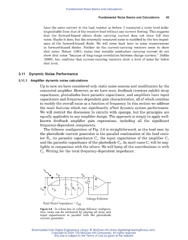
The follower configuration of Fig. 3.8 is straightforward, as the load seen by
the photodiode current generator is the parallel combination of the load resis-
tor R L, its parasitic capacitance C s, the input capacitance of the amplifier C i,
and the parasitic capacitance of the photodiode C p. In most cases C s will be neg-
ligible in comparison with the others. We will lump all the contributions in with
C p. Writing for the total frequency-dependent impedance:
I p e n
i n
V b C p C s R L C i
Voltage Follower
Total Shunt Impedance = Z sh
Figure 3.8 In a bias box or voltage follower configura-
tion, noise can be estimated by placing all stray and
input capacitances in parallel with the photodiode
current generator.
Downloaded from Digital Engineering Library @ McGraw-Hill (www.digitalengineeringlibrary.com)
Copyright © 2004 The McGraw-Hill Companies. All rights reserved.
Any use is subject to the Terms of Use as given at the website.