
Page 67 - Photodetection and Measurement - Maximizing Performance in Optical Systems
P. 67
Fundamental Noise Basics and Calculations
60 Chapter Three
Z sh = RZ Cp (3.17)
L
R L + Z Cp
Z Cp = 1/sC p is the impedance of the total parasitic capacitance, and s = j2pf is
the complex angular frequency. Appendix A gives some pointers on the use of
the complex frequency to calculate such electrical networks. The signal output
is just I p Z sh. (This signal shows a low-pass characteristic, starting at I pR L at a
low frequency, before reducing above the break frequency 1/2pR LC p.)
The amplifier’s current noise generator flows similarly through the shunt
impedance Z sh, so that both photocurrent and current noise contributions at the
amplifier output exhibit the same low-pass characteristic. The voltage noise
density generator’s output simply appears at the amplifier output and is essen-
tially independent of frequency. Above some frequency it will therefore domi-
nate the noise density. If the voltage noise contribution is negligible, then S/N
is constant with frequency.
The easiest way to treat the thermal noise of the load resistor is to consider
(
it as another current source 4 R kW) pA Hz in parallel with the photocur-
rent and shot noise sources. All three current sources then show the same low-
pass characteristic due to the falling shunt impedance Z sh.
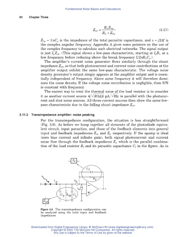
3.11.2 Transimpedance amplifier: noise peaking
For the transimpedance configuration, the situation is less straightforward
(Fig. 3.9). As before we lump together all elements of the photodiode equiva-
lent circuit, input parasitics, and those of the feedback elements into general
input and feedback impedances Z sh and Z f, respectively. If the opamp is ideal
(zero bias current and infinite gain), both signal photocurrent and current
noise flow through the feedback impedance Z f, which is the parallel combina-
tion of the load resistor R f and its parasitic capacitance C f in the figure. As in
Z f
C f
R f
I p e n
i n
C p R sh C i
Z sh
Figure 3.9 The transimpedance configuration can
be analyzed using the total input and feedback
impedances.
Downloaded from Digital Engineering Library @ McGraw-Hill (www.digitalengineeringlibrary.com)
Copyright © 2004 The McGraw-Hill Companies. All rights reserved.
Any use is subject to the Terms of Use as given at the website.