
Page 313 - Power Electronics Handbook
P. 313
Inverter circuits 303
r
c
Three phase load
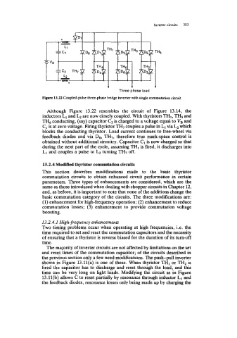
Figure 13.22 Coupled-pulse three-phase bridge inverter with single commutation circuit
Although Figure 13.22 resembles the circuit of Figure 13.14, the
inductors L1 and b are now closely coupled. With thyristors TH1, TH5 and
TI& conducting, (say) capacitor C2 is charged to a voltage equal to VB and
C1 is at zero voltage. Firing thyristor TH7 couples a pulse in L1 via which
blocks the conducting thyristor. Load current continues to free-wheel via
feedback diodes and via Dg, TH7, therefore true mark-space control is
obtained without additional circuitry. Capacitor C1 is now charged so that
during the next part of the cycle, assuming TH, is fired, it discharges into
L1 and couples a pulse to b turning TH7 off.
13.2.4 Modified thyristor commutation circuits
This section describes modifications made to the basic thyristor
commutation circuits to obtain enhanced circuit performance in certain
parameters. Three types of enhancements are considered, which are the
same as those introduced when dealing with chopper circuits in Chapter 12,
and, as before, it is important to note that none of the additions change the
basic commutation category of the circuits. The three modifications are:
(1) enhancement for high-frequency operation; (2) enhancement to reduce
commutation losses; (3) enhancement to provide commutation voltage
boosting.
13.2.4.1 High-frequency enhancements
Two timing problems occur when operating at high frequencies, i.e. the
time required to set and reset the commutation capacitors and the necessity
of ensuring that a thyristor is reverse biased for the duration of its turn-off
time.
The majority of inverter circuits are not affected by limitations on the set
and reset times of the commutation capacitor; of the circuits described in
the previous section only a few need modifications. The push-pull inverter
shown in Figure 13.11(a) is one of these. When thyristor TH1 or TH2 is
fired the capacitor has to discharge and reset through the load, and this
time can be very long on light loads. Modifying the circuit as in Figure
13.11(b) allows C to reset partially by resonance through inductor L1 and
the feedback diodes, resonance losses only being made up by charging the