
Page 317 - Power Electronics Handbook
P. 317
Inverter circuits 307
13.2.4.2 Commutation loss reduction
Commutation losses can be reduced, as was done for choppers, by several
techniques. For example, Figure 13.1 l(b) illustrated a popular push-pull
parallel commutated inverter configuration, which is not suitable for
high-frequency operation due to its large commutation loss. When TH1
fires, capacitor C discharges through inductor L1 and recharges to twice the
supply voltage. When this has been completed diode D1 conducts, feeding
back the inductive load current to the supply, and the energy stored in L1
during the commutation interval is dissipated in the loop L1-D1-TH1.
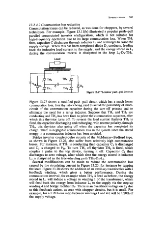
Load
D2
Figure 13.27 ‘Lossless’ push-pull inverter
Figure 13.27 shows a modified push-pull circuit which has a much lower
commutation loss, four thyristors being used to avoid the possibility of short-
circuit of the commutation capacitor during the turn-off process and to
eliminate the need for a series inductor. Suppose that TH, and TH3 are
conducting and TH, has been fired to prime the commutation capacitor, after
which this thyristor turns off. To reverse the load current thyristor TH, is
fired, the capacitor discharging and recharging, with reverse polarity, through
TH3, this thyristor also going off when the capacitor has completed its
charge. There is negligible commutation loss in the system since the stored
energy in a commutation inductor has been avoided.
Bridge inverter coupled-pulse circuits of the McMurray-Bedford typ,
as shown in Figure 13.20, also suffer from relatively high commutation
losses. For instance, if TH1 is conducting then capacitor C1 is discharged
and C, is charged to VB. To turn TH1 off thyristor TH2 is fired, which
couples a pulse to the top device, turning it off. Capacitor C, then
discharges to zero voltage, after which time the energy stored in inductor
L1 is dissipated in the free-wheeling path TH2-D2-L1.
Several modifications can be made to reduce the commutation loss
caused by the circulating current in Figure 13.20, for instance by tapping
the load. Figure 13.28 shows the addition of an auxiliary transformer with a
feedback winding, which gives a better performance. During the
commutation interval, for example when THz is fired as before, the energy
stored in L1 will induce a voltage in winding 1 of the transformer, which
will feed back the energy from inductor L1 to the supply via the step-up
winding 4 and bridge rectifier D7. There is an overshoot voltage on due
to this feedback action, as seen with chopper circuits, but it is small. For
example, for a 1:20 turns ratio between windings 1 and 4 it will be 1/20th of
the supply voltage.