
Page 264 - Power Electronics Handbook
P. 264
254 Forced commutation techniques
(iii) The capacitor voltage is increased by the load current, as before,
being given by equation (11.7), since on heavy loads most of the
capacitor discharge will occur through the load.
(iv) If commutation fails for any reason then it cannot be re-attempted
since the main thyristor, being continuously on, prevents the
capacitor from charging with plate b positive.
(v) The rating of the main thyristor is increased by the capacitor resonant
current.
(vi) No low-impedance fault current path exists across the supply.
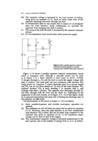
Figure 11.10 A parallel capacitor-inductor
commutated circuit capable of variable
frequency and variable mark-space operation
Figure 11.10 shows a parallel capacitor-inductor commutation circuit
which is frequently used. ,Although a saturable reactor can be used,
as in Figure 11.9, a linear inductor is more usual, as shown. Initially
C charges through L1, D3 and the load to reach the supply voltage with
plate b positive. The load cycle can now commence with thyristor THI
being turned on. Capacitor C cannot discharge since D3 is reverse biased
and TH2 has not yet been turned on. To turn off the main thyristor TH1
auxiliary thyristor TH2 is fired, enabling C to resonate with L1 and
recharge with plate a positive. The capacitor now discharges through D3
and then through both the load and the diode D2, depending on the
magnitude of the load current, as in Figure 11.9. As in that figure, diode
D2 optional and performs the same role of limiting the discharge time of
is
the capacitor on light loads.
The performance of the circuit in Figure 11.10 is as follows:
(i) Both variable-frequency and variable mark-space operation are
possible.
(ii) The minimum on and off times are equal and are given by equation
(11.3). However, since the main thyristor is not now commutated
until thyristor TH2 is fired, this can be made long compared to the
resonant time given in equation (11.3), so the maximum output
voltage can be close to that of the supply.
(iii) The commutation capacitor voltage is increased proportional to the
load current, due to the transfer of energy from L1 to C, as before,