
Page 195 - Radar Technology Encyclopedia
P. 195
185 filter characteristics filter, coherent [circulating] memory
mable CCD transversal filters are constructed both with con-
trol relative to the phase and amplitude of signals at delay line
x(t) h(t) y(t) taps and with control only relative to phase. In the first
S (j ) w H(j ) w S (j ) w instance, great universality is achieved; while, in the second,
y
x
the base of the processed signal is maximized. For an N-stage
filter, maximum base magnitude equals N/2 (N for a sin-
Figure F25 Generic two-port filter.
gle-crystal filter reaches 512). IAM
impulse response is the time response to an impulse input (d- Ref.: Brodersen, R. W., et al. IEEE Trans., ED-23, no. 2, 1976, p. 143;
Hague, Y. A., and Copeland, M. A., IEEE J. Solid-State Circuits, SC-12,
function). The transfer function is a complex quantity:
1977.
jfw()
=
Hjw( ) H w()e × Chebyshev filter (see frequency-selective filter).
a
where H(w) and f(w)re called the amplitude-frequency A coherent integration [comb] filter is a narrowband filter
response and the phase-frequency response, respectively. The at IF or baseband that is matched to a specific target doppler
complex transfer function H(jw) is often termed the fre- frequency and whose response repeats at the pulse repetition
quency response. The functions h(t) and H(jw) are a Fourier frequency. Typically this repeated (comb) response is
transform pair, and if they are known, the output signal and its obtained by range-gating the input signal at the input to a nar-
spectrum can be found as rowband filter. In search and target acquisition radar modes, a
filter bank covering all doppler frequencies within the pulse
yt () xt () ht ()Ä
=
repetition frequency interval is usually implemented (by fast
Fourier transform or similar techniques) to detect a target at
(
S jw( ) S jw )Hjw )
=
×
(
y x
any velocity. This filter bank is an essential part of the mov-
where Ä is the notation for the convolution operation. For ing target detector or pulsed doppler types of signal process-
deterministic signals, S(jw) is the signal spectrum, and for ing. In tracking radars and homing seekers, a single filter (or
random signals, it is a signal power spectrum. velocity gate) may be used, tracking the target doppler fre-
In the case of a digital filter, the transfer function H (jw) quency.
d
becomes a periodic function, because the signal sampling at Coherent integrating filters are necessarily doppler sensi-
time intervals Dt: tive, the passband of each filter being inversely proportional
¥ to the integration time. The difficulty in direct synthesis of
2p
æ
–
×
H jw( ) = å Hj w n ------ ö comb filters in the frequency domain leads to the approach in
Dt ø
è
d
n = – ¥ which the signal is sampled in range gates (or with range
strobes, for digital filters), before passing into a bandpass fil-
In terms of the z-transform the transfer function of a digital
ter or bank of such filters. DKB
filter can be represented as
Ref.: Skolnik (1980), pp. 121–125; Barton (1988), pp. 253–264; Schleher
Az ()
=
Hz () ----------- (1991), pp. 10, 73–103.
Bz ()
The values giving A(z) = 0 are called filter zeroes, and those The coherent [circulating] memory filter is an analog pro-
giving B(z) = 0 are called filter poles. The choice of filter cessing circuit in which an IF signal is recirculated n times
zeroes and poles permits design of filters with the required through a delay line, with a frequency shift that is the recipro-
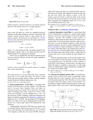
transfer function for different applications. SAL cal of the pulse length (Fig. F26). The effect is to form, within
Ref.: Fink (1982), Ch. 12; Gol’denberg (1985). each pulse width at the output, a series of time responses cor-
responding to doppler filters formed during the n-pulse inte-
A charge-coupled-device (CCD) filter is an analog filter
gration period. This is one form of coherent integration filter.
having a CCD delay line as its basic element. CCD filters are
used as low-pass filters, bandpass filters, and filters for
matched processing of signals with a large base. The band- IF signal out
IF signal in Delay line
width of a bandpass filter at the -3-dB level is 1.04 to 1.08% S Filter
(1/PRF)
of the carrier frequency, and the sidelobe level is -38 to -42
dB. Selection of filter weighting coefficients determines the
Single-
degree of sidelobe suppression (for Hamming weighting, the sideband
mixer Oscillator
sidelobe level is -42.8 dB). The advantage of CCD bandpass f = 1/ t
filters over others is the ease in changing their resonant fre- Clutter signal Aircraft signal
quency over a broad range achieved by adjusting the clock
frequency.
Programmable transversal CCD filters are widely used Time (range)
t t
for matched filtering. Signal processing in CCD filters occurs
in the video frequency for a bandwidth from zero to half the Figure F26 Coherent memory filter block diagram and output
clock frequency, which does not exceed 20 MHz. Program- signal (after Skolnik, 1970, Figs. 62, 63, pp. 17.56–17.57).