
Page 148 - Rashid, Power Electronics Handbook
P. 148
136 B. M. Wilamowski
anode anode
p +
p +
pnp
pnp
n -
n - C
gate p p p SIT
n +
gate p npn
n + cathode (a) (b)
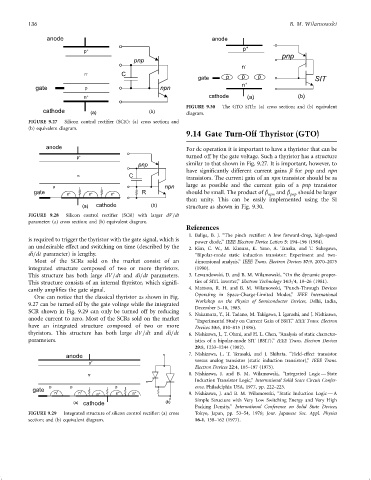
FIGURE 9.30 The GTO SITh: (a) cross section; and (b) equivalent
cathode (a) (b) diagram.
FIGURE 9.27 Silicon control recti®er (SCR): (a) cross section; and
(b) equivalent diagram.
9.14 Gate Turn-Off Thyristor (GTO)
anode For dc operation it is important to have a thyristor that can be
p + turned off by the gate voltage. Such a thyristor has a structure
pnp similar to that shown in Fig. 9.27. It is important, however, to
have signi®cantly different current gains b for pnp and npn
n - C
transistors. The current gain of an npn transistor should be as
p npn large as possible and the current gain of a pnp transistor
gate n + n + n + R should be small. The product of b npn and b pnp should be larger
than unity. This can be easily implemented using the SI
(a) cathode (b) structure as shown in Fig. 9.30.
FIGURE 9.28 Silicon control recti®er (SCR) with larger dV=dt
parameter: (a) cross section; and (b) equivalent diagram.
References
1. Baliga, B. J. ‘‘The pinch recti®er: A low forward-drop, high-speed
is required to trigger the thyristor with the gate signal, which is
power diode,'' IEEE Electron Device Letters 5: 194–196 (1984).
an undesirable effect and switching on time (described by the 2. Kim, C. W., M. Kimura, K. Yano, A. Tanaka, and T. Sukegawa,
di=dt parameter) is lengthy. ‘‘Bipolar-mode static induction transistor: Experiment and two-
Most of the SCRs sold on the market consist of an dimensional analysis,'' IEEE Trans. Electron Devices 37:9, 2070–2075
integrated structure composed of two or more thyristors. (1990).
This structure has both large dV=dt and di=dt parameters. 3. Lewandowski, D. and B. M. Wilamowski, ‘‘On the dynamic proper-
This structure consists of an internal thyristor, which signi®- ties of SITL inverter,'' Electron Technology 14:3=4, 19–26 (1981).
cantly ampli®es the gate signal. 4. Mattson, R. H. and B. M. Wilamowski, ‘‘Punch-Through Devices
Operating in Space-Charge-Limited Modes,'' IEEE International
One can notice that the classical thyristor as shown in Fig.
Workshop on the Physics of Semiconductor Devices, Delhi, India,
9.27 can be turned off by the gate voltage while the integrated
December 5–10, 1983.
SCR shown in Fig. 9.29 can only be turned off by reducing
5. Nakamura, Y., H. Tadano, M. Takigawa, I. Igarashi, and J. Nishizawa,
anode current to zero. Most of the SCRs sold on the market ‘‘Experimental Study on Current Gain of BSIT,'' IEEE Trans. Electron
have an integrated structure composed of two or more Devices 33:6, 810–815 (1986).
thyristors. This structure has both large dV=dt and di=dt 6. Nishizawa, J., T. Ohmi, and H. L. Chen, ‘‘Analysis of static character-
parameters. istics of a bipolar-mode SIT (BSIT),'' IEEE Trans. Electron Devices
29:8, 1233–1244 (1982).
anode 7. Nishizawa, J., T. Terasaki, and J. Shibata, ‘‘Field-effect transistor
versus analog transistor (static induction transistor),'' IEEE Trans.
p +
Electron Devices 22:4, 185–197 (1975).
n - 8. Nishizawa, J. and B. M. Wilamowski, ‘‘Integrated Logic Ð State
Induction Transistor Logic,'' International Solid State Circuit Confer-
p p p ence, Philadelphia USA, 1977, pp. 222–223.
gate
n + n + n + n + n + 9. Nishizawa, J. and B. M. Wilamowski, ‘‘Static Induction Logic Ð A
(a) cathode (b) Simple Structure with Very Low Switching Energy and Very High
Packing Density,'' International Conference on Solid State Devices,
FIGURE 9.29 Integrated structure of silicon control recti®er: (a) cross Tokyo, Japan, pp. 53–54, 1976; Jour. Japanese Soc. Appl. Physics
section; and (b) equivalent diagram. 16-1, 158–162 (1977).