Page 143 - Rashid, Power Electronics Handbook
P. 143

9 Static Induction Devices                                                                          131

                                                                      much narrower potential barrier can be obtained when other
                                                                      types of emitter are used. There are two well-known emitters:
                                                                      (1) p-n junction (Fig. 9.10a); and (2) Schottky junction (Fig.
                                                                      9.10b). For silicon devices p-n junctions have a forward
                                                                      voltage drop of 0.7–0.8 V while Schottky emitters have 0.2–
                                                                      0.3 V only. As the Schottky diode is a majority carrier device,
                                                                      carrier storage effect is negligible.
                                                                        Another interesting emitter structure is shown in Fig. 9.10c.
                                                                      This emitter has all the advantages of the Schottky diode even
                                                                      though it is fabricated out of p-n junctions.
                                                                        The concept of static induction devices can be used inde-
                                                                      pendently of the type of emitter shown in Fig. 9.10. With
                                                                      Schottky type and punch-through type emitters the poten-
                                                                      tial barrier is much narrower and this results in faster response
                                                                      time and larger current gain in the bipolar mode of
                                                                      operation.


                                                                      9.6 Static Induction Diode (SID)

                                                                      The bipolar mode of operation of SIT also can be used to
                                                                      obtain diodes with low forward voltage drop and negligible
                                                                      carrier storage effect [2, 5, 13, 23, 24]. A static induction diode
                                                                      can be obtained by shorting a gate to the emitter of the static
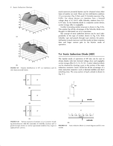
                 FIGURE 9.9  Potential distributions in SIT: (a) traditional; and (b)  induction transistor. Such a diode has all the advantages of a
                 with sharp potential barrier.                        static induction transistor such as thermal stability and short
                                                                      switching time. The cross section of such a diode is shown in
                                                                      Fig. 9.11.


                                    p         n -


                                                                                       SIT
                                     (a)


                                              n -
                                                                                (a)
                                                                                                     anode

                                     (b)                                                      n +


                                    n +  p    n -                                             n -

                                                                                     p   p   p   p   p   p
                                                                                            emitter
                                     (c)
                                                                                                     cathode
                 FIGURE 9.10  Various structures of emitters: (a) p-n junction includ-
                                                                                (b)
                 ing heterostructure with SiGe materials; (b) Schottky junction; and (c)
                 punch-through emitter (in normal operational condition the p region is  FIGURE 9.11  Static induction diode: (a) circuit diagram; and (b) cross
                 depleted from carriers).                             section.
   138   139   140   141   142   143   144   145   146   147   148