Page 142 - Rashid, Power Electronics Handbook
P. 142

130                                                                                    B. M. Wilamowski

               9.4 Bipolar Mode Operation of SI devices               I
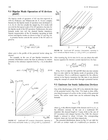
                                                                       DS
                    (BSIT)                                            [mA]

               The bipolar mode of operation of SIT was ®rst reported in
               1976 by Nishizawa and Wilamowski [8, 9]. Several complex  100
               theories for the bipolar mode of operation were developed [2,
               5, 6, 10, 23, 24], but actually the simple Eq. (9.5) works well  =50m A
               not only for the typical mode of the SIToperation, but also for    40m A  30m A  20m A  10m A  5m A  2m A  =0
                                                                               I  G
               the bipolar mode of the SIT operation. Furthermore, the same                                 I  G
               formula works very well for classical bipolar transistors.
               Typical characteristics of the SI transistor operating in both  50
               normal and bipolar modes are shown in Figs. 9.7 and Fig. 9.8.
                 A potential barrier controls the current in the SIT and it is
               given by


                                        qD N S
                                          n
                              n
                              J ¼ „  x 2                     ð9:13Þ
                                     expðÿjðxÞ=V Þdx                                2         4         4  V   [V]
                                   x 1          T                                                            DS
                                                                    FIGURE 9.8  Small-sized SIT transistor characteristic, operating in
               where jðxÞ is the pro®le of the potential barrier along the  both normal and bipolar modes, I D ¼ f ðV DS Þ with I G as a parameter.
               channel.
                 For example, in the case of npn bipolar transistors the  After inserting Eq. (9.14) into (9.13) one can obtain the well-
               potential distribution across the base in reference to emitter  known equation for electron current injected into the base
               potential at the reference impurity level N ¼ N is described
                                                  E    S
               by:                                                                      qD n 2       V BE
                                                                                           n i
                                                                                  J ¼ „         exp               ð9:15Þ
                                                                                   n   x 2
                                                                                         N ðxÞdx    V T
                                                                                          B
                                                                                       x 1

                                     N ðxÞN S       V BE
                                      B
                         jðxÞ¼ V ln      2    exp ÿ          ð9:14Þ   If Eq. (9.13) is valid for SIT and BJT then one may assume
                                 T
                                        n           V
                                         i           T
                                                                    that it is also valid for the bipolar mode of operation of the
                                                                    SIT transistor. This is a well-known equation for the collector
                                                                    current in the bipolar transistor, but this time it was derived
                  I                                                 using the concept of current ¯ow through a potential barrier.
                   DS   V =0.75V
                  [mA]    GS
                                V =0.7V                             9.5 Emitters for Static Induction Devices
                                 GS
                                          V =0.65V
                                           GS                       One of the disadvantages of the SIT is the relatively ¯at shape
                                                                    of the potential barrier (Fig. 9.9a). This leads to slow, diffu-
                   100
                                                                    sion-based transport of carriers in the vicinity of the potential
                                           0.6V                     barrier. The carrier transit time can be estimated using the
                                                                    formula:
                                               0.5V 0.4V
                                                                                                2
                    50                            0.3V 0V                                t transit  ¼  l eff      ð9:16Þ
                                                    -0.5V -1V                                   D
                                                     -2V            where l eff  is the effective length of the channel and D ¼ mV is
                                                                                                                   T
                                                     -3V            the diffusion constant. In the case of a traditional SIT
                                                                    transistor this channel length is  2 mm, while in the case of
                                                                    SIT transistors with sharper barriers (Fig. 9.9b) the channel
                                                                    length is reduced to about  0:2 mm. The corresponding
                                  2         4           V   [V]
                                                         DS         transient times are 2 ns and 20 ps respectively.
               FIGURE 9.7  Small-sized SIT transistor characteristic, operating in  The potential distributions shown in Fig. 9.3 are valid for
               both normal and bipolar modes, I D ¼ f ðV DS Þ with V GS as parameter.  SIT with an emitter made of a traditional p-n junction. A
   137   138   139   140   141   142   143   144   145   146   147