
Page 140 - Rashid, Power Electronics Handbook
P. 140
128 B. M. Wilamowski
source Note that the preceding equations derived for SIT also can
be used to ®nd current in any devices controlled by a potential
n +
barrier, such as a bipolar transistor or a MOS transistor
n - n - operating in subthreshold mode, or in a Schottky diode.
p + p + p + p + p + gate
n -
9.3 Characteristics of Static Induction
Transistor
n +
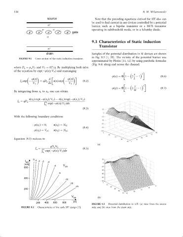
drain Samples of the potential distribution in SI devices are shown
in Fig. 9.3 [1, 20]. The vicinity of the potential barrier was
FIGURE 9.1 Cross section of the static induction transistor.
approximated by Plotka [11, 12] by using parabolic formulas
(Fig. 9.4) along and across the channel.
where D ¼ m V and V ¼ kT=q. By multiplying both sides
n
T
T
n
of the equation by expðÿjðxÞ=V Þ and rearranging
T
x 2
jðxÞ¼ F 1 ÿ 2 ÿ 1 ð9:6Þ
jðxÞ d jðxÞ L
J exp ÿ ¼ qD n nðxÞ exp ÿ ð9:2Þ
n
V dx V
T T
y 2
jðyÞ¼ F 1 ÿ 2 ÿ 1 ð9:7Þ
By integrating from x to x , one can obtain W
1 2
nðx Þ expðÿjðx Þ=V Þÿ nðx Þ expðÿjðx Þ=V Þ
T
1
2
1
T
2
J ¼ qD n x 2
n
expðÿjðxÞ=V Þdx
T
x 1
ð9:3Þ
With the following boundary conditions
jðx Þ¼ 0; nðx Þ¼ N ;
1 1 S
ð9:4Þ
jðx Þ¼ V ; nðx Þ¼ N ;
2 D 2 D
Equation (9.3) reduces to
(a)
qD N S
n
n
J ¼ x 2 ð9:5Þ
expðÿjðxÞ=V Þdx
x 1 T
0
I -1 -2 -3
DS -4
[mA]
-6 V GS
600
-8
400
-15
-20
-25
200
V
DS (b)
200 400 600 800 [V]
FIGURE 9.3 Potential distribution in SIT: (a) view from the source
FIGURE 9.2 Characteristics of the early SIT design [7]. side; and (b) view from the drain side.