
Page 144 - Rashid, Power Electronics Handbook
P. 144
132 B. M. Wilamowski
SIT
n + n + n +
p p
p - p -
Schotty Drain Gate Emitter Gate Drain
(a)
(a)
n + n + n +
p + p p +
n - n -
p p p p p
Drain Gate Emitter Gate Drain
(b)
n -
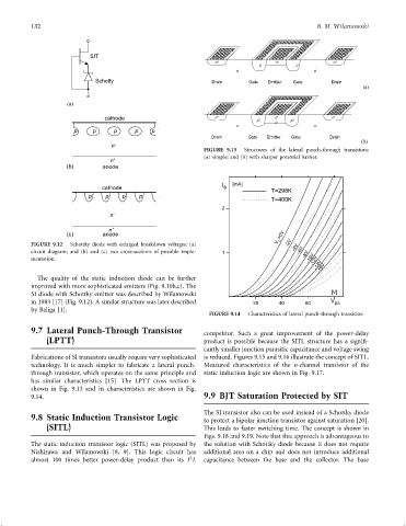
FIGURE 9.13 Structures of the lateral punch-through transistors:
(a) simple; and (b) with sharper potential barrier.
n +
(b) anode
I [mA]
cathode D
T=298K
p p p p
T=400K
2
n -
n +
(c) anode V G =0V
FIGURE 9.12 Schottky diode with enlarged breakdown voltages: (a) -2V -4V
circuit diagram; and (b) and (c) two cross-sections of possible imple- 1 -6V -8V
mentation. -10V -12V -14V -16V
The quality of the static induction diode can be further
improved with more sophisticated emitters (Fig. 9.10b,c). The
SI diode with Schottky emitter was described by Wilamowski [V]
in 1983 [17] (Fig. 9.12). A similar structure was later described 20 40 60 V DS
by Baliga [1].
FIGURE 9.14 Characteristics of lateral punch-through transistor.
9.7 Lateral Punch-Through Transistor competitor. Such a great improvement of the power-delay
(LPTT) product is possible because the SITL structure has a signi®-
cantly smaller junction parasitic capacitance and voltage swing
Fabrications of SI transistors usually require very sophisticated is reduced. Figures 9.15 and 9.16 illustrate the concept of SITL.
technology. It is much simpler to fabricate a lateral punch- Measured characteristics of the n-channel transistor of the
through transistor, which operates on the same principle and static induction logic are shown in Fig. 9.17.
has similar characteristics [15]. The LPTT cross section is
shown in Fig. 9.13 and its characteristics are shown in Fig.
9.14. 9.9 BJT Saturation Protected by SIT
The SI transistor also can be used instead of a Schottky diode
9.8 Static Induction Transistor Logic to protect a bipolar junction transistor against saturation [20].
(SITL) This leads to faster switching time. The concept is shown in
Figs. 9.18 and 9.19. Note that this approach is advantageous to
The static induction transistor logic (SITL) was proposed by the solution with Schottky diode because it does not require
Nishizawa and Wilamowski [8, 9]. This logic circuit has additional area on a chip and does not introduce additional
2
almost 100 times better power-delay product than its I L capacitance between the base and the collector. The base