
Page 147 - Rashid, Power Electronics Handbook
P. 147
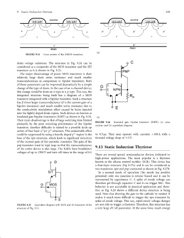
9 Static Induction Devices                                                                          135

                                       source                                                 source
                            poly gate              poly gate                      poly gate             poly gate
                         n +        n +         n +        n +                n +         n +        n +        n  +
                                                                               p                     p          p
                    p                     p                     p         p +                   p +                 p +

                               n -                     n -                          n -                    n -

                                          n +                                                   p +
                                        drain                                                drain
                                                                       (a)
                       FIGURE 9.24  Cross section of the DMOS transistor.


                 drain voltage variations. The structure in Fig. 9.24 can be                  C
                 considered as a composite of the MOS transistor and the SIT
                 transistor as it is shown in Fig. 9.25.                                PNP
                   The major disadvantage of power MOS transistors is their
                 relatively large drain series resistance and much smaller
                 transconductance in comparison to bipolar transistors. Both
                 of these parameters can be improved dramatically by a simple
                 change of the type of drain. In the case of an n-channel device,  G  NPN
                 this change would be from an n-type to a p-type. This way, the
                 integrated structure being built has a diagram of a MOS                     R
                 transistor integrated with a bipolar transistor. Such a structure             P
                 has b times larger transconductance (b is the current gain of a
                 bipolar transistor) and much smaller series resistance due to      E
                 the conductivity modulation effect caused by holes injected
                 into the lightly doped drain region. Such devices are known as
                 insulated gate bipolar transistors (IGBT) as shown in Fig. 9.26.  (b)
                 Their main disadvantage is that of large switching time limited
                                                                      FIGURE 9.26  Insulated gate bipolar transistor (IGBT): (a) cross
                 primarily by the poor switching performance of the bipolar
                                                                      section; and (b) equivalent diagram.
                 transistor. Another dif®culty is related to a possible latch-up
                                     ÿ þ
                                  þ
                 action of four layer n pn p -structure. This undesirable effect
                                                       þ
                 could be suppressed by using a heavily doped p -region in the  to 0.5 ms. They may operate with currents >100 A with a
                 base of the npn structure, which leads to signi®cant reduction  forward voltage drop of  3V.
                 of the current gain of this parasitic transistor. The gain of the
                 pnp transistor must be kept large so that the transconductance  9.13 Static Induction Thyristor
                 of the entire device is also large. The IGBTs have breakdown
                 voltages of up to 1500 V and turn-off times in the range of 0.1
                                                                      There are several special semiconductor devices dedicated to
                                                                      high-power applications. The most popular is a thyristor
                                           D                          known as the silicon control recti®er (SCR). This device has
                                                                      a four-layer structure (Fig 9.27a) and it can be considered as
                                                                      two transistors npn and pnp connected as shown in Fig. 9.27b.
                                      SIT                               In a normal mode of operation (the anode has positive
                                                                      potential) only one junction is reverse biased and it can be
                                                                      represented by capacitance C. A spike of anode voltage can
                                                                      therefore get through capacitor C and it can trigger SRC. This
                                 G     MOS
                                                                      behavior is not acceptable in practical application and there-
                                                                      fore as Fig. 9.28 shows a different device structure is being
                                                                      used. Note that shorting the gate to the cathode by resistor R
                                                                      makes it much more dif®cult to trigger the npn transistor by
                                             S
                                                                      spike of anode voltage. This way, rapid anode voltage changes
                 FIGURE 9.25  Equivalent diagram with MOS and SI transistors of the  are not able to trigger a thyristor. Therefore, this structure has
                 structure of Fig. 9.24.                              a very large dV=dt parameter. At the same time, much energy