
Page 145 - Rashid, Power Electronics Handbook
P. 145
9 Static Induction Devices 133
B E C
p p n + p n + p n + n + n +
p
n - p n - p
n -
n + n + n +
FIGURE 9.15 Cross section of SIT logic. p p
FIGURE 9.19 Cross sections of bipolar transistors protected against
deep saturation using SIT.
supply
current collector capacitance is always enlarged by the Miller effect and
this leads to slower switching in the case of the solution with
out1 out2 out3 the Schottky diode.
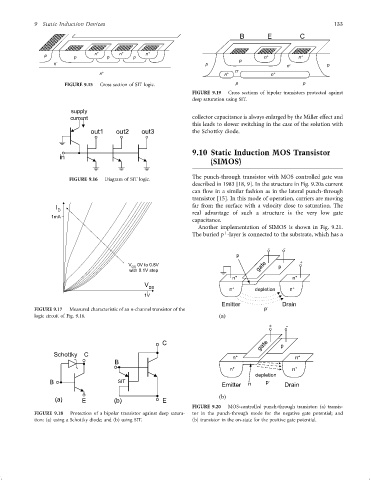
9.10 Static Induction MOS Transistor
in
(SIMOS)
The punch-through transistor with MOS controlled gate was
FIGURE 9.16 Diagram of SIT logic.
described in 1983 [18, 9]. In the structure in Fig. 9.20a current
can ¯ow in a similar fashion as in the lateral punch-through
transistor [15]. In this mode of operation, carriers are moving
I far from the surface with a velocity close to saturation. The
D
real advantage of such a structure is the very low gate
1mA
capacitance.
Another implementation of SIMOS is shown in Fig. 9.21.
þ
The buried p -layer is connected to the substrate, which has a
- -
p
V 0V to 0.8V +
GS gate p
with 0.1V step
n + n +
V
DS + +
n depletion n
1V
Emitter Drain
FIGURE 9.17 Measured characteristic of an n-channel transistor of the p -
logic circuit of Fig. 9.16. (a)
+ -
gate p
C
Schottky C
n + n +
B
n + n +
depletion
B SIT p -
Emitter n Drain
(b)
(a) E (b) E
FIGURE 9.20 MOS-controlled punch-through transistor: (a) transis-
FIGURE 9.18 Protection of a bipolar transistor against deep satura- tor in the punch-through mode for the negative gate potential; and
tion: (a) using a Schottky diode; and (b) using SIT. (b) transistor in the on-state for the positive gate potential.