
Page 146 - Rashid, Power Electronics Handbook
P. 146
134 B. M. Wilamowski
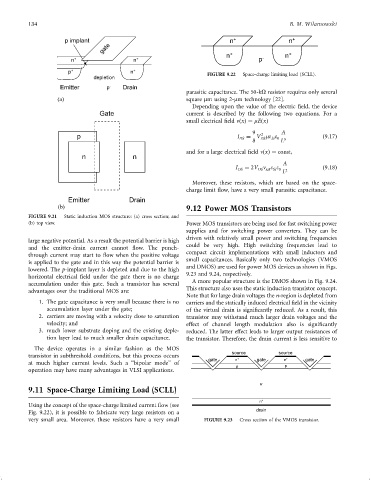
p implant n + n +
gate
n + - n +
n + n + p
p + n + FIGURE 9.22 Space-charge limiting load (SCLL).
depletion
Emitter p - Drain
parasitic capacitance. The 50-kO resistor requires only several
(a) square mm using 2-mm technology [22].
Depending upon the value of the electric ®eld, the device
Gate current is described by the following two equations. For a
small electrical ®eld nðxÞ¼ mEðxÞ
9 A
2
p I DS ¼ V me e ð9:17Þ
Si 0
DS
8 L 3
and for a large electrical ®eld nðxÞ¼ const,
n n
A
I ¼ 2V n e e ð9:18Þ
DS DS sat Si 0 2
L
Moreover, these resistors, which are based on the space-
charge limit ¯ow, have a very small parasitic capacitance.
Emitter Drain
(b) 9.12 Power MOS Transistors
FIGURE 9.21 Static induction MOS structure: (a) cross section; and
(b) top view. Power MOS transistors are being used for fast switching power
supplies and for switching power converters. They can be
driven with relatively small power and switching frequencies
large negative potential. As a result the potential barrier is high
could be very high. High switching frequencies lead to
and the emitter-drain current cannot ¯ow. The punch-
through current may start to ¯ow when the positive voltage compact circuit implementations with small inductors and
is applied to the gate and in this way the potential barrier is small capacitances. Basically only two technologies (VMOS
and DMOS) are used for power MOS devices as shown in Figs.
lowered. The p-implant layer is depleted and due to the high
9.23 and 9.24, respectively.
horizontal electrical ®eld under the gate there is no charge
A more popular structure is the DMOS shown in Fig. 9.24.
accumulation under this gate. Such a transistor has several
This structure also uses the static induction transistor concept.
advantages over the traditional MOS are:
Note that for large drain voltages the n-region is depleted from
1. The gate capacitance is very small because there is no carriers and the statically induced electrical ®eld in the vicinity
accumulation layer under the gate; of the virtual drain is signi®cantly reduced. As a result, this
2. carriers are moving with a velocity close to saturation transistor may withstand much larger drain voltages and the
velocity; and effect of channel length modulation also is signi®cantly
3. much lower substrate doping and the existing deple- reduced. The latter effect leads to larger output resistances of
tion layer lead to much smaller drain capacitance. the transistor. Therefore, the drain current is less sensitive to
The device operates in a similar fashion as the MOS
source source
transistor in subthreshold conditions, but this process occurs
gate n + gate n + gate
at much higher current levels. Such a ‘‘bipolar mode'' of
p p
operation may have many advantages in VLSI applications.
n -
9.11 Space-Charge Limiting Load (SCLL)
n +
Using the concept of the space-charge limited current ¯ow (see
Fig. 9.22), it is possible to fabricate very large resistors on a drain
very small area. Moreover, these resistors have a very small FIGURE 9.23 Cross section of the VMOS transistor.