Page 141 - Rashid, Power Electronics Handbook
P. 141

9 Static Induction Devices                                                                          129

                                                       W                       0 -2  -4  -6
                                                                          I           -8  -10
                                                                           DS
                                                        F                 [mA]                -12    -14
                                       2F
                             F                                            500                              -16

                            L                                             400
                                                                                                               V =-18
                                                                                                                G
                                                                          300
                 FIGURE 9.4  Potential distribution in the vicinity of the barrier
                 approximated by parabolic shapes.                        200

                                                                          100
                   Integrating Eq. (9.5) ®rst along the channel and then across                                 V DS
                 the channel yields a very simple formula for drain currents in                                [V]
                                                                                  20   40   60   80   100  120
                 n-channel SIT transistors
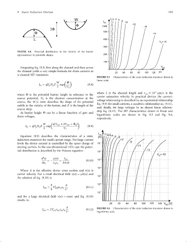
                                                                      FIGURE 9.5  Characteristics of the static induction transistor drawn in
                                                                      linear scale.

                                           W      F
                                I ¼ qD N Z    exp               ð9:8Þ
                                D
                                      p
                                         S
                                            L     V T
                                                                                                            11
                                                                      where L is the channel length and n    10 mm=s is the
                 where F is the potential barrier height in reference to the                          sat
                                                                      carrier saturation velocity. In practical devices the current-
                 source potential, N S  is the electron concentration at the  voltage relationship is described by an exponential relationship
                 source, the W=L ratio describes the shape of the potential
                                                                      Eq. (9.9) for small currents, a quadratic relationship eq. (9.11),
                 saddle in the vicinity of the barrier, and Z is the length of the
                                                                      and, ®nally, for large voltages by an almost linear relation-
                 source strip.
                                                                      ship Eq. (9.12). The SIT characteristics drawn in linear and
                   As barrier height F can be a linear function of gate and
                                                                      logarithmic scales are shown in Fig. 9.5 and Fig. 9.6,
                 drain voltages,
                                                                      respectively.

                                  W      aðV GS  þ bV DS  þ F Þ
                                                        0
                       I ¼ qD N Z    exp                        ð9:9Þ
                                S
                       D
                             p
                                   L            V T
                                                                       I DS  0 -1 -2
                   Equation (9.9) describes the characteristics of a static  [A]  -3 -4  -5  -6
                 induction transistor for small current range. For large current      -7
                                                                                            -9
                 levels the device current is controlled by the space charge of  10 -1
                                                                                                 -11
                 moving carriers. In the one-dimensional (1D) case the poten-
                 tial distribution is described by the Poisson equation:  10 -2                       -13
                                                                                                              V =-15
                                                                                                               G
                                  2
                                 d j     rðxÞ   I DS                    -3
                                     ¼ÿ      ¼                 ð9:10Þ  10
                                  dx 2   e e   AnðxÞ
                                          Si 0
                                                                      10 -4
                   Where A is the effective device cross section and nðxÞ is
                 carrier velocity. For a small electrical ®eld nðxÞ¼ mEðxÞ and
                                                                      10 -5
                 the solution of Eq. (9.10) is
                                        9  2     A                    10 -6
                                  I DS  ¼ V me e               ð9:11Þ
                                              Si 0
                                          DS
                                        8        L 3
                                                                      10 -7
                 and for a large electrical ®eld nðxÞ¼ const and Eq. (9.10)
                 results in:
                                                                              20    40   60    80   100  120  140 V   [V]
                                                                                                                   DS
                                                  A                   FIGURE 9.6  Characteristics of the static induction transistor drawn in
                                  I DS  ¼ 2V n e e             ð9:12Þ
                                         DS sat Si 0
                                                 L 2                  logarithmic scale.
   136   137   138   139   140   141   142   143   144   145   146