
Page 223 - Rashid, Power Electronics Handbook
P. 223
212 D. Czarkowski
understood and described in the literature. Advantages of
PWM converters include low component count, high ef®-
ciency, constant frequency operation, relatively simple control
and commercial availability of integrated circuit controllers,
and ability to achieve high conversion ratios for both step-
down and step-up application. A disadvantage of PWM dc-dc
converters is that PWM rectangular voltage and current wave-
forms cause turn-on and turn-off losses in semiconductor
devices, which limit practical operating frequencies to
hundreds of kilohertz. Rectangular waveforms also inherently
generate EMI.
This chapter begins with a section on dc choppers that are
used primarily in dc drives. The output voltage of dc choppers
is controlled by adjusting the on time of a switch, which in
turn adjusts the width of a voltage pulse at the output. This is
the so-called pulse width modulation (PWM) control. The dc
choppers with additional ®ltering components form PWM dc-
dc converters. Four basic dc-dc converter topologies are
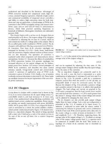
presented in Sections 13.3–13.6 Ð buck, boost, buck-boost, FIGURE 13.1 DC chopper with resistive load: (a) circuit diagram; (b)
Á
and Cuk converters. Popular isolated versions of these conver- output voltage waveform.
ters are also discussed. The operation of converters is
where T ¼ 1=f is the period of the switching frequency f . The
explained under ideal component and semiconductor device
average value of the output voltage is
assumptions. Section 13.7 discusses the effects of nonidealities
in PWM converters; Section 13.8 presents topologies for
V ¼ DV S ð13:2Þ
O
increased ef®ciency at low output voltages and for bidirec-
tional power ¯ow; Section 13.9 reviews control principles of and can be regulated by adjusting the duty ratio D. The
PWM dc-dc converters, and describes two main control average output voltage is always smaller than the input voltage,
schemes, namely, voltage-mode control and current-mode hence the name of the converter.
control. A summary of application areas of PWM dc-dc The dc step-down choppers are commonly used in dc
converters is given in Section 13.10. Finally, a list of modern drives. In such a case, the load is represented as a series
textbooks on power electronics is provided [1–8]. These books combination of inductance L, resistance R, and back-emf E as
are excellent resources for deeper exploration of the area of dc- shown in Fig. 13.2a. To provide a path for a continuous
dc power conversion. inductor current ¯ow when the switch is in the off state, an
antiparallel diode D must be connected across the load.
Because the chopper of Fig. 13.2a provides a positive voltage
13.2 DC Choppers and a positive current to the load, it is called a ®rst-quadrant
chopper. The load voltage and current are graphed in Fig.
13.2b under assumptions that the load current never reaches
A step-down dc chopper with a resistive load is shown in Fig.
zero and the load time constant t ¼ L=R is much greater than
13.1a. It is a series connection of a dc input voltage source V , the period T. Average values of the output voltage and current
S
controllable switch S, and load resistance R. In most cases, can be adjusted by changing the duty ratio D.
switch S has unidirectional voltage-blocking capabilities and The dc choppers can also provide peak output voltages
unidirectional current-conduction capabilities. Power electro- higher than the input voltage. Such a step-up con®guration is
nic switches are usually implemented with power MOSFETs,
presented in Fig. 13.3. It consists of dc input source V ,
S
IGBTs, MCTs, power BJTs, or GTOs. If an antiparallel diode is
inductor L connected in series with the source, switch S
used or embedded in a switch, the switch exhibits a bidirec-
connecting the inductor to ground, and a series combination
tional current conduction property. Figure 13.1b depicts wave-
of diode D and load. If the switch operates with a duty ratio D,
forms in a step-down chopper. The switch is being operated
the output voltage is a series of pulses of duration ð1 ÿ DÞT
with a duty ratio D de®ned as a ratio of the switch on time to
and amplitude V =ð1 ÿ DÞ. Therefore, neglecting losses, the
S
the sum of the on and off times. For a constant frequency
average value of the output voltage is V . To obtain an average
S
operation
value of the output voltage greater than V , a capacitor must
S
be connected in parallel with the load. This results in a
t on t on
D ¼ ð13:1Þ topology of a boost dc-dc converter that is described in
t on þ t off T Section 13.4.