
Page 225 - Rashid, Power Electronics Handbook
P. 225
214 D. Czarkowski
It can be seen from Eq. (13.4) that the output voltage is always by the effects of parasitic components in the converter,
smaller that the input voltage. especially by the equivalent series resistance of the capacitor.
The dc-dc converters can operate in two distinct modes Parasitic components in dc-dc converters are discussed in
with respect to the inductor current i . Figure 13.4b depicts Section 13.7.
L
the CCM in which the inductor current is always greater than
zero. When the average value of the output current is low 13.3.2 Transformer Versions of Buck Converter
(high R) and=or the switching frequency f is low, the conver-
ter may enter the discontinuous conduction mode (DCM). In In many dc power supplies, a galvanic isolation between the dc
the DCM, the inductor current is zero during a portion of the or ac input and the dc output is required for safety and
switching period. The CCM is preferred for high ef®ciency and reliability. An economical means of achieving such an isolation
good utilization of semiconductor switches and passive is to employ a transformer version of a dc-dc converter. High-
components. The DCM may be used in applications with frequency transformers are of a small size and low weight and
special control requirements because the dynamic order of the provide high ef®ciency. Their turns ratio can be used addi-
converter is reduced (the energy stored in the inductor is zero tionally to adjust the output voltage level. Among buck-
at the beginning and at the end of each switching period). It is derived dc-dc converters, the most popular are the forward
uncommon to mix these two operating modes because of converter, the push-pull converter, the half-bridge converter,
different control algorithms. For the buck converter, the value and the full-bridge converter.
of the ®lter inductance that determines the boundary between
CCM and DCM is given by 13.3.2.1 Forward Converter
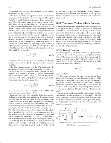
The circuit diagram of a forward converter is depicted in Fig.
ð1 ÿ DÞR
L ¼ ð13:5Þ 13.5. When the switch S is on, diode D conducts and diode
1
b
2f D is off. The energy is transferred from the input, through the
2
transformer, to the output ®lter. When the switch is off, the
For typical values of D ¼ 0:5, R ¼ 10 O, and f ¼ 100 kHz, the state of diodes D and D is reversed. The dc voltage transfer
2
1
boundary is L ¼ 25 mH. For L > L , the converter operates in function of the forward converter is
b
b
the CCM.
The ®lter inductor current i in the CCM consists of a dc D
L
component I with a superimposed triangular ac component. M ¼ n ð13:7Þ
V
O
Almost all of this ac component ¯ows through the ®lter
capacitor as a current i . Current i causes a small voltage where n ¼ N =N .
c
c
1
2
ripple across the dc output voltage V . To limit the peak-to- In the forward converter, the energy-transfer current ¯ows
O
peak value of the ripple voltage below a certain value V , the through the transformer in one direction. Hence, an addi-
r
®lter capacitance C must be greater than tional winding with diode D is needed to bring the magnetiz-
3
ing current of the transformer to zero, which prevents
ð1 ÿ DÞV O transformer saturation. The turns ratio N =N should be
C min ¼ ð13:6Þ 1 3
8V Lf 2
r selected in such a way that the magnetizing current decreases
to zero during a fraction of the time interval when the switch
At D ¼ 0:5, V =V ¼ 1%, L ¼ 25 mH, and f ¼ 100 kHz, the
r O is off.
minimum capacitance is C min ¼ 25 mF. Equations (13.5) and (13.6) can be used to design the ®lter
Equations (13.5) and (13.6) are the key design equations for components. The forward converter is very popular for low-
the buck converter. The input and output dc voltages (hence, power applications. For medium-power levels, converters with
the duty ratio D), and the range of load resistances R are bidirectional transformer excitation (push-pull, half-bridge,
usually determined by preliminary speci®cations. The designer and full-bridge) are preferred due to better utilization of
needs to determine values of passive components L and C, and magnetic components.
of the switching frequency f . The value of the ®lter inductor L
is calculated from the CCM=DCM condition using Eq. (13.5).
The value of the ®lter capacitor C is obtained from the voltage
ripple condition Eq. (13.6). For the compactness and low
conduction losses of a converter, it is desirable to use small
passive components. Equations (13.5) and (13.6) show that it
can be accomplished by using a high switching frequency f .
The switching frequency is limited, however, by the type of
semiconductor switches used and by switching losses. It
should also be noted that values of L and C may be altered FIGURE 13.5 Forward converter.