
Page 224 - Rashid, Power Electronics Handbook
P. 224
13 DC-DC Converters 213
FIGURE 13.2 DC chopper with RLE load: (a) circuit diagram;
(b) waveforms.
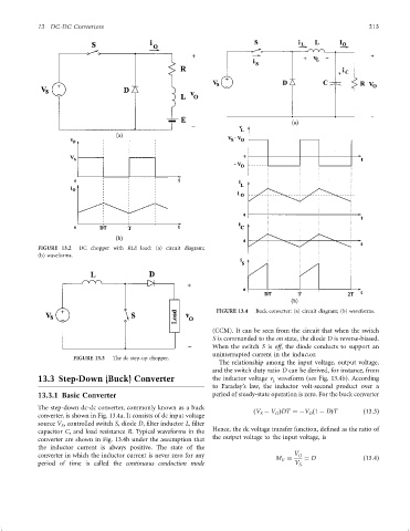
FIGURE 13.4 Buck converter: (a) circuit diagram; (b) waveforms.
(CCM). It can be seen from the circuit that when the switch
S is commanded to the on state, the diode D is reverse-biased.
When the switch S is off, the diode conducts to support an
uninterrupted current in the inductor.
FIGURE 13.3 The dc step-up chopper.
The relationship among the input voltage, output voltage,
and the switch duty ratio D can be derived, for instance, from
13.3 Step-Down (Buck) Converter the inductor voltage v waveform (see Fig. 13.4b). According
L
to Faraday's law, the inductor volt-second product over a
13.3.1 Basic Converter period of steady-state operation is zero. For the buck converter
The step-down dc-dc converter, commonly known as a buck ðV ÿ V ÞDT ¼ÿV ð1 ÿ DÞT ð13:3Þ
converter, is shown in Fig. 13.4a. It consists of dc input voltage S O O
source V , controlled switch S, diode D, ®lter inductor L, ®lter
S
capacitor C, and load resistance R. Typical waveforms in the Hence, the dc voltage transfer function, de®ned as the ratio of
converter are shown in Fig. 13.4b under the assumption that the output voltage to the input voltage, is
the inductor current is always positive. The state of the
converter in which the inductor current is never zero for any V O
M ¼ D ð13:4Þ
V
period of time is called the continuous conduction mode V S