
Page 227 - Rashid, Power Electronics Handbook
P. 227
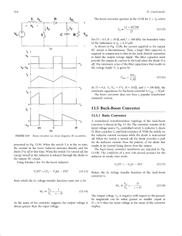
216                                                                                        D. Czarkowski

                                                                      The boost converter operates in the CCM for L > L where
                                                                                                                b
                                                                                                 2
                                                                                           ð1 ÿ DÞ DR
                                                                                      L ¼                        ð13:15Þ
                                                                                       b
                                                                                              2f
                                                                    For D ¼ 0:5, R ¼ 10 O, and f ¼ 100 kHz, the boundary value
                                                                    of the inductance is L ¼ 6:25 mH.
                                                                                      b
                                                                      As shown in Fig. 13.9b, the current supplied to the output
                                                                    RC circuit is discontinuous. Thus, a larger ®lter capacitor is
                                                                    required in comparison to that in the buck-derived converters
                                                                    to limit the output voltage ripple. The ®lter capacitor must
                                                                    provide the output dc current to the load when the diode D is
                                                                    off. The minimum value of the ®lter capacitance that results in
                                                                    the voltage ripple V is given by
                                                                                    r
                                                                                              DV O
                                                                                        C   ¼                    ð13:16Þ
                                                                                         min
                                                                                              V Rf
                                                                                                r
                                                                    At D ¼ 0:5, V =V ¼ 1%, R ¼ 10 O, and f ¼ 100 kHz, the
                                                                                   O
                                                                                r
                                                                    minimum capacitance for the boost converter is C min  ¼ 50 mF.
                                                                      The boost converter does not have a popular transformer
                                                                    (isolated) version.

                                                                    13.5 Buck-Boost Converter


                                                                    13.5.1 Basic Converter
                                                                    A nonisolated (transformerless) topology of the buck-boost
                                                                    converter is shown in Fig. 13.10a. The converter consists of dc
                                                                    input voltage source V , controlled switch S, inductor L, diode
                                                                                      S
                                                                    D, ®lter capacitor C, and load resistance R. With the switch on,
                FIGURE 13.9  Boost converter: (a) circuit diagram; (b) waveforms.  the inductor current increases while the diode is maintained
                                                                    off. When the switch is turned off, the diode provides a path
                                                                    for the inductor current. Note the polarity of the diode that
               presented in Fig. 13.9b. When the switch S is in the on state,
                                                                    results in its current being drawn from the output.
               the current in the boost inductor increases linearly and the
                                                                      The buck-boost converter waveforms are depicted in Fig.
               diode D is off at that time. When the switch S is turned off, the
                                                                    13.10b. The condition of a zero volt-second product for the
               energy stored in the inductor is released through the diode to
                                                                    inductor in steady state yields
               the output RC circuit.
                 Using Faraday's law for the boost inductor
                                                                                    V DT ¼ÿV ð1 ÿ DÞT            ð13:17Þ
                                                                                     S        O
                             V DT ¼ðV ÿ V Þð1 ÿ DÞT         ð13:13Þ
                              S       O    S                        Hence, the dc voltage transfer function of the buck-boost
                                                                    converter is
               from which the dc voltage transfer function turns out to be
                                                                                          V O      D
                                                                                    M        ¼ÿ                  ð13:18Þ
                                                                                      V   V      1 ÿ D
                                      V O    1                                              S
                                 M       ¼                  ð13:14Þ
                                   V
                                       V S  1 ÿ D
                                                                    The output voltage V is negative with respect to the ground.
                                                                                     O
                                                                    Its magnitude can be either greater or smaller (equal at
               As the name of the converter suggests, the output voltage is  D ¼ 0:5) than the input voltage as the name of the converter
               always greater than the input voltage.               implies.