
Page 231 - Rashid, Power Electronics Handbook
P. 231
220 D. Czarkowski
capacitance, the maximum value of the peak-to-peak ripple
voltage across the capacitance is
V Cmax V ÿ V rc ð13:35Þ
r
Finally, by analogy to Eq. (13.16), when the ESR of the ®lter
capacitor is taken into account in the boost-type output ®lter,
the ®lter capacitance should be greater than
DV O
C min ¼ ð13:36Þ
V Cmax Rf
Parasitic resistances, capacitances, and voltage sources also
affect the energy conversion ef®ciency of dc-dc converters. The
ef®ciency Z is de®ned as a ratio of output power to the input
power
P O V I
O O
Z ¼ ð13:37Þ
P V I
S S S
Thus as ef®ciencies are usually speci®ed in percent, let us
consider the boost converter as an example. Under the low
ripple assumption, the boost converter ef®ciency can be
estimated as
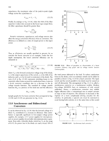
2
Rð1 ÿ DÞ
Z ¼ 2 ð13:38Þ FIGURE 13.14 Effects of parasitics on characteristics of a boost
Rð1 ÿ DÞ ð1 þ V =V þ fC RÞ
D O o converter: ef®ciency (top graph) and dc voltage transfer function
þr þ Dr þð1 ÿ DÞr þ Dð1 ÿ DÞr C (bottom graph).
L
D
S
where V is the forward conduction voltage drop of the diode,
D
C is the output capacitance of the switch, r is the ESR of the the total power delivered to the load. To reduce conduction
L
o
inductor, and r is the forward on resistance of the diode. The losses in the diode, a low on-resistance switch can be added in
D
term fC R in Eq. (13.38) represents switching losses in the parallel as shown in Fig. 13.15 for a buck converter. The input
o
converter; other terms account for conduction losses. Losses in switch and the switch parallel to the diode must be turned on
a dc-dc converter contribute also to a decrease in the dc and off alternately. The arrangement of Fig. 13.15 is called a
voltage transfer function. The nonideal dc voltage transfer synchronous converter or a synchronous recti®er. Modern
function M Vn is a product of the ideal one and the ef®ciency low-voltage MOSFETs have on resistances of only several
milliohms. Hence, a synchronous converter may exhibit
M Vn ¼ ZM V ð13:39Þ higher ef®ciency than a conventional one at output currents
as large as tens of amperes. The ef®ciency is increased at the
Sample graphs for the boost converter that correspond to Eqs. expense of a more complicated driving circuitry for the
(13.38) and (13.39) are presented in Fig. 13.14. switches. In particular, a special care must be exercised to
avoid having both switches on at the same time as this would
13.8 Synchronous and Bidirectional
Converters
It can be observed in Eq. (13.38) that the forward voltage of a
diode V contributes to a decrease in ef®ciency. This contri-
D
bution is especially signi®cant in low-output voltage power
supplies, for example, 3.3-V power supplies for microproces-
sors or power supplies for portable telecommunication equip-
ment. Even with a Schottky diode, which has V in the range
D
of 0:4 V, the power loss in the diode can easily exceed 10% of FIGURE 13.15 Synchronous buck converter.