
Page 228 - Rashid, Power Electronics Handbook
P. 228
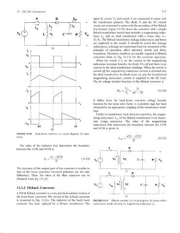
13  DC-DC Converters                                                                                217

                                                                      input dc source V and switch S are connected in series with
                                                                                     S
                                                                      the transformer primary. The diode D and the RC output
                                                                      circuit are connected in series with the secondary of the ¯yback
                                                                      transformer. Figure 13.11b shows the converter with a simple
                                                                      ¯yback transformer model that includes a magnetizing induc-
                                                                      tance L m  and an ideal transformer with a turns ratio n ¼
                                                                      N /N . The ¯yback transformer leakage inductances and losses
                                                                          2
                                                                       1
                                                                      are neglected in the model. It should be noted that leakage
                                                                      inductances, although not important from the viewpoint of the
                                                                      principle of operation, affect adversely switch and diode
                                                                      transitions. Therefore, snubbers are usually required in ¯yback
                                                                      converters Refer to Fig. 13.11b for the converter operation.
                                                                        When the switch S is on, the current in the magnetizing
                                                                      inductance increases linearly, the diode D is off and there is no
                                                                      current in the ideal transformer windings. When the switch is
                                                                      turned off, the magnetizing inductance current is diverted into
                                                                      the ideal transformer, the diode turns on, and the transformed
                                                                      magnetizing inductance current is supplied to the RC load.
                                                                      The dc voltage transfer function of the ¯yback converter is

                                                                                            V O     D
                                                                                      M        ¼                   ð13:20Þ
                                                                                        V
                                                                                            V S  nð1 ÿ DÞ
                                                                      It differs from the buck-boost converter voltage transfer
                                                                      function by the turns ratio factor n. A positive sign has been
                                                                      obtained by an appropriate coupling of the transformer wind-
                                                                      ings.
                                                                        Unlike in transformer buck-derived converters, the magne-
                                                                      tizing inductance L of the ¯yback transformer is an impor-
                                                                                      m
                                                                      tant design parameter. The value of the magnetizing
                                                                      inductance that determines the boundary between the CCM
                                                                      and DCM is given by
                 FIGURE 13.10  Buck-boost converter: (a) circuit diagram; (b) wave-                  2
                                                                                              2
                                                                                             n ð1 ÿ DÞ R
                 forms.
                                                                                       L mb  ¼                     ð13:21Þ
                                                                                                 2f
                   The value of the inductor that determines the boundary
                 between the CCM and DCM is

                                               2
                                         ð1 ÿ DÞ R
                                    L ¼                       ð13:19Þ
                                     b
                                            2f
                 The structure of the output part of the converter is similar to
                 that of the boost converter (reversed polarities are the only
                 difference). Thus, the value of the ®lter capacitor can be
                 obtained from Eq. (13.16).

                 13.5.2 Flyback Converter

                 A PWM ¯yback converter is a very practical isolated version of
                 the buck-boost converter. The circuit of the ¯yback converter
                 is presented in Fig. 13.11a. The inductor of the buck-boost  FIGURE 13.11  Flyback conveter: (a) circuit diagram; (b) circuit with a
                 converter has been replaced by a ¯yback transformer. The  transformere model showing the magnetizing inductance L m .