Page 254 - Rashid, Power Electronics Handbook
P. 254

14  Inverters                                                                                       243

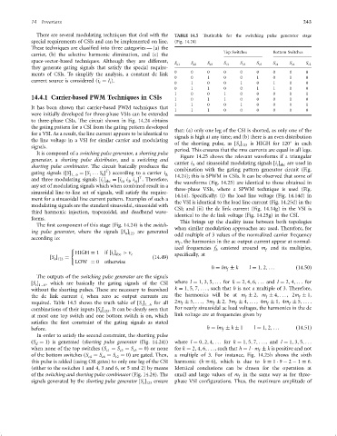
                   There are several modulating techniques that deal with the  TABLE 14.5  Truthtable for the switching pulse generator stage
                 special requirements of CSIs and can be implemented on line.  (Fig. 14.24)
                 These techniques are classi®ed into three categories Ð (a) the
                                                                                        Top Switches      Bottom Switches
                 carrier, (b) the selective harmonic elimination, and (c) the
                 space-vector-based techniques. Although they are different,
                                                                      S a1  S a2  S a3  S c1  S c3  S c5  S c4  S c6  S c2
                 they generate gating signals that satisfy the special require-
                                                                      0     0     0     0     0     0     0     0     0
                 ments of CSIs. To simplify the analysis, a constant dc link
                                                                      0     0     1     0     0     1     0     1     0
                 current source is considered (i ¼ I ).               0     1     0     0     1     0     1     0     0
                                              i
                                          i
                                                                      0     1     1     0     0     1     1     0     0
                                                                      1     0     0     1     0     0     0     0     1
                 14.4.1 Carrier-based PWM Techniques in CSIs          1     0     1     1     0     0     0     1     0
                                                                      1     1     0     0     1     0     0     0     1
                 It has been shown that carrier-based PWM techniques that
                                                                      1     1     1     0     0     0     0     0     0
                 were initially developed for three-phase VSIs can be extended
                 to three-phase CSIs. The circuit shown in Fig. 14.24 obtains
                 the gating pattern for a CSI from the gating pattern developed  that: (a) only one leg of the CSI is shorted, as only one of the
                 for a VSI. As a result, the line current appears to be identical to  signals is high at any time; and (b) there is an even distribution
                 the line voltage in a VSI for similar carrier and modulating  of the shorting pulse, as ‰S Š  is HIGH for 120 in each

                                                                                             e 123
                 signals.                                             period. This ensures that the rms currents are equal in all legs.
                   It is composed of a switching pulse generator,a shorting pulse
                                                                        Figure 14.25 shows the relevant waveforms if a triangular
                 generator,a shorting pulse distributor, and a switching and
                                                                      carrier i and sinusoidal modulating signals ‰i Š  are used in
                                                                            D
                                                                                                           c abc
                 shorting pulse combinator. The circuit basically produces the  combination with the gating pattern generator circuit (Fig.
                                             T
                 gating signals ð‰SŠ  ¼‰S ... S Š Þ according to a carrier i
                                1...6  1   6                       D  14.24); this is SPWM in CSIs. It can be observed that some of
                                                         T
                 and three modulating signals ‰i Š  ¼‰i i i Š . Therefore,
                                           c abc  ca cb ca            the waveforms (Fig. 14.25) are identical to those obtained in
                 any set of modulating signals which when combined result in a
                                                                      three-phase VSIs, where a SPWM technique is used (Fig.
                 sinusoidal line-to-line set of signals, will satisfy the require-
                                                                      14.14). Speci®cally: (i) the load line voltage (Fig. 14.14d) in
                 ment for a sinusoidal line current pattern. Examples of such a
                                                                      the VSI is identical to the load line current (Fig. 14.25d) in the
                 modulating signals are the standard sinusoidal, sinusoidal with
                                                                      CSI; and (ii) the dc link current (Fig. 14.14g) in the VSI is
                 third harmonic injection, trapezoidal, and deadband wave-
                                                                      identical to the dc link voltage (Fig. 14.25g) in the CSI.
                 forms.
                                                                        This brings up the duality issue between both topologies
                   The ®rst component of this stage (Fig. 14.24) is the switch-
                                                                      when similar modulation approaches are used. Therefore, for
                 ing pulse generator, where the signals ‰S Š  are generated  odd multiple of 3 values of the normalized carrier frequency
                                                    a 123
                 according to:
                                                                      m , the harmonics in the ac output current appear at normal-
                                                                        f
                                                                      ized frequencies f centered around m and its multiples,
                                (                                                    h                 f
                                  HIGH ¼ 1  if ‰i Š  > v c            speci®cally, at
                                               c abc
                        ‰S Š  ¼                               ð14:49Þ
                          a 123
                                  LOW ¼ 0   otherwise
                                                                                   h ¼ lm   k    l ¼ 1; 2; ...     ð14:50Þ
                                                                                         f
                   The outputs of the switching pulse generator are the signals
                 ‰S Š  , which are basically the gating signals of the CSI  where l ¼ 1; 3; 5; ... for k ¼ 2; 4; 6; ... and l ¼ 2; 4; ... for
                   c 1...6
                 without the shorting pulses. These are necessary to freewheel  k ¼ 1; 5; 7; ... , such that h is not a multiple of 3. Therefore,
                 the dc link current i when zero ac output currents are  the harmonics will be at m   2, m   4; ... ,2m   1,
                                                                                                                    f
                                                                                                       f
                                                                                                f
                                    i
                 required. Table 14.5 shows the truth table of ‰S Š  for all  2m   5; ... ,3m   2, 3m   4; ... ,4m   1, 4m   5; ... .
                                                                                    f
                                                                         f
                                                                                                        f
                                                                                            f
                                                                                                                f
                                                          c 1...6
                 combinations of their inputs ‰S ‰  . It can be clearly seen that  For nearly sinusoidal ac load voltages, the harmonics in the dc
                                           a 123
                 at most one top switch and one bottom switch is on, which  link voltage are at frequencies given by
                 satis®es the ®rst constraint of the gating signals as stated
                 before.                                                          h ¼ lm   k   1   l ¼ 1; 2; ...   ð14:51Þ
                                                                                        f
                   In order to satisfy the second constraint, the shorting pulse
                 ðS ¼ 1Þ is generated (shorting pulse generator (Fig. 14.24))  where l ¼ 0; 2; 4; ... for k ¼ 1; 5; 7; ..., and l ¼ 1; 3; 5; ...
                   d
                 when none of the top switches ðS ¼ S ¼ S ¼ 0Þ or none  for k ¼ 2; 4; 6; ..., such that h ¼ l   m   k is positive and not
                                             c1
                                                       c5
                                                                                                     f
                                                  c3
                 of the bottom switches ðS ¼ S ¼ S ¼ 0Þ are gated. Then,  a multiple of 3. For instance, Fig. 14.25h shows the sixth
                                                c2
                                      c4
                                           c6
                 this pulse is added (using OR gates) to only one leg of the CSI  harmonic ðh ¼ 6Þ, which is due to h ¼ 1   9 ÿ 2 ÿ 1 ¼ 6.
                 (either to the switches 1 and 4, 3 and 6, or 5 and 2) by means  Identical conclusions can be drawn for the operation at
                 of the switching and shorting pulse combinator (Fig. 14.24). The  small and large values of m in the same way as for three-
                                                                                             f
                 signals generated by the shorting pulse generator ‰S Š  ensure  phase VSI con®gurations. Thus, the maximum amplitude of
                                                          e 123
   249   250   251   252   253   254   255   256   257   258   259