Page 252 - Rashid, Power Electronics Handbook
P. 252

14  Inverters                                                                                       241

                                                                      which is not singular and hence

                                                                                                   ÿ1
                                                                             2    3   2           3 2     3
                                                                               v an     1  ÿ1    0     v ab
                                                                             6    7   6           7 6     7
                                                                                bn      0   1  ÿ1 5 4  v 5
                                                                                                        bc
                                                                               v 5 ¼ 4
                                                                             4
                                                                               v cn     1   1    1      0
                                                                                                                   ð14:47Þ
                                                                                       2           32    3
                                                                                           2   1  1    v ab
                                                                                      1 6          76    7
                                                                                                       bc
                                                                                                     4
                                                                                    ¼ 4  ÿ1    1  1 5 v 5
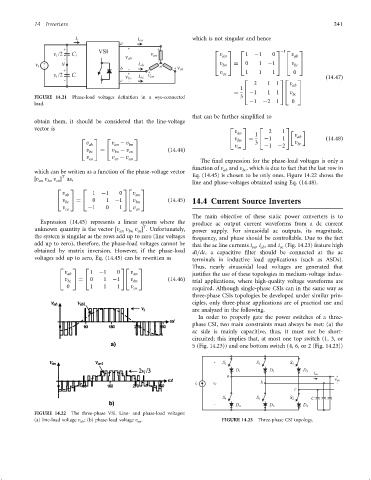
                 FIGURE 14.21  Phase-load voltages de®nition in a wye-connected       3
                                                                                         ÿ1   ÿ2  1    0
                 load.
                                                                      that can be further simpli®ed to
                 obtain them, it should be considered that the line-voltage
                 vector is                                                        2    3    2        3
                                                                                    v an   1    2   1    v
                                 2   3   2         3                              4  v bn  5  ¼  4  ÿ1  1  5  ab   ð14:48Þ
                                   v       v ÿ v                                           3            v bc
                                    ab      an   bn                                 v cn      ÿ1  ÿ2
                                 4  v bc  5  ¼  4  v ÿ v cn  5  ð14:44Þ
                                            bn
                                   v ca    v ÿ v an
                                            cn
                                                                         The ®nal expression for the phase-load voltages is only a
                                                                      function of v and v , which is due to fact that the last row in
                                                                                ab
                                                                                       bc
                 which can be written as a function of the phase-voltage vector  Eq. (14.45) is chosen to be only ones. Figure 14.22 shows the
                           T
                 ‰v  v  v Š as,
                   an  bn  cn                                         line and phase-voltages obtained using Eq. (14.48).
                         2   3   2             32    3
                           v ab      1  ÿ1    0   v an
                         4  v bc  5  ¼  4  0  1  ÿ1  54 v bn  5  ð14:45Þ  14.4 Current Source Inverters
                           v ca    ÿ1    0    1   v cn
                                                                      The main objective of these static power converters is to
                   Expression (14.45) represents a linear system where the  produce ac output current waveforms from a dc current
                                                      T
                 unknown quantity is the vector ‰v an  v bn  v Š . Unfortunately,  power supply. For sinusoidal ac outputs, its magnitude,
                                                    cn
                 the system is singular as the rows add up to zero (line voltages  frequency, and phase should be controllable. Due to the fact
                 add up to zero), therefore, the phase-load voltages cannot be  that the ac line currents i , i , and i (Fig. 14.23) feature high
                                                                                                   oc
                                                                                          oa
                                                                                             ob
                 obtained by matrix inversion. However, if the phase-load  di=dt, a capacitive ®lter should be connected at the ac
                 voltages add up to zero, Eq. (14.45) can be rewritten as  terminals in inductive load applications (such as ASDs).
                                                                      Thus, nearly sinusoidal load voltages are generated that
                          2   3   2           32    3
                            v ab    1  ÿ1    0   v an                 justi®es the use of these topologies in medium-voltage indus-
                          4  v bc  5  ¼  4  0  1  ÿ1  54 v bn  5  ð14:46Þ  trial applications, where high-quality voltage waveforms are
                            0       1    1   1    v cn                required. Although single-phase CSIs can in the same way as
                                                                      three-phase CSIs topologies be developed under similar prin-
                                                                      ciples, only three-phase applications are of practical use and
                                                                      are analyzed in the following.
                                                                        In order to properly gate the power switches of a three-
                                                                      phase CSI, two main constraints must always be met: (a) the
                                                                      ac side is mainly capacitive, thus, it must not be short-
                                                                      circuited; this implies that, at most one top switch (1, 3, or
                                                                      5 (Fig. 14.23)) and one bottom switch (4, 6, or 2 (Fig. 14.23))


                 FIGURE 14.22  The three-phase VSI. Line- and phase-load voltages:
                 (a) line-load voltage v ab ; (b) phase-load voltage v an .     FIGURE 14.23  Three-phase CSI topology.
   247   248   249   250   251   252   253   254   255   256   257