
Page 34 - Rashid, Power Electronics Handbook
P. 34
18 A. I. Maswood
safety factor to cater to these overvoltages, that is, a diode
with a 220 2 1:5 ¼ 660 V rating.
2.4.2 Current Ratings
Power diodes are usually mounted on a heat sink. This
effectively dissipates the heat arising due to continuous
conduction. Current ratings are estimated based on tempera-
ture rise considerations. The data sheet of a diode normally
speci®es three different current ratings. These are: (1) the
average current; (2) the rms current; and (3) the peak current.
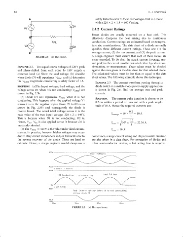
FIGURE 2.5 (a) The circuit. A design engineer must ensure that each of these values are
never exceeded. To do that, the actual current (average, rms,
and peak) in the circuit must be evaluated either by calculation,
EXAMPLE 2.2. Two equal source voltages of 220 V peak simulation, or measurement. These values must be checked
and phase-shifted from each other by 180 supply a against the ones given in the data sheet for that selected diode.
common load: (a) Show the load voltage; (b) describe The calculated values must be less than or equal to the data
when diode D1 will experience V RRM ; and (c) determine sheet values. The following example shows this technique.
the V RRM magnitude considering a safety factor of 1.5. EXAMPLE 2.3 The current waveform passing through a
SOLUTION. (a)The Input voltages, load voltage, and the diode switch in a switch-mode power-supply application
voltage across D1 when it is not conducting (V RRM ) are is shown in Fig. 2.6. Find the average, rms and peak
shown in Fig. 2.5b. currents.
(b) Diode D1 will experience V when it is not
RRM SOLUTION. The current pulse duration is shown to be
conducting. This happens when the applied voltage V1
0.2 ms within a period of 1 ms and with a peak ampli-
across it is in the negative region (from 70 to 80 ms as
tude of 50 A. Hence the required currents are:
shown in Fig. 2.5b) and consequently the diode is
reverse biased. The actual ideal voltage across it is the 0:2
I ¼ 50 ¼ 10 A
peak value of the two input voltages 220 2 ¼ 440 V. average 1
This is because when D1 is not conducting, D2 is. r
0:2
Hence, V ; V bn is also applied across it because D2is I rms ¼ 50 ¼ 22:36 A
2
an
practically shorted. 1
(c) The V RRM ¼ 440 V is the value under ideal circum- I rms ¼ 50 A
stances. In practice, however, higher voltages may occur
due to stray circuit inductances and=or transients due to Sometimes, a surge current rating and its permissible duration
the reverse recovery of the diode. These are hard to are also given in a data sheet. For protection of diodes and
estimate. Hence, a design engineer would always use a other semiconductor devices, a fast acting fuse is required.
FIGURE 2.5 (b) The waveforms.