
Page 38 - Rashid, Power Electronics Handbook
P. 38
22 A. I. Maswood
ol 2 2 2
where a ¼ a tan ; and Z ¼ R þ ol
R
ÿRy E
iðyÞ¼ A*e þ sinðy ÿ aÞ ð2:9Þ
ol Z
E
A ¼ sinðaÞ ð2:10Þ
Z
Hence, the average output voltage:
E ð b E
V OAVG ¼ sin y:dy ¼ *1 ÿ cosðbÞ ð2:11Þ
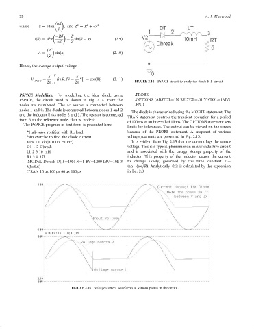
2p 0 2p FIGURE 2.14 PSPICE circuit to study the diode R-L circuit.
PSPICE Modelling: For modelling the ideal diode using .PROBE
PSPICE, the circuit used is shown in Fig. 2.14. Here the .OPTIONS (ABSTOL¼1N RELTOL¼.01 VNTOL¼1MV)
nodes are numbered. The ac source is connected between .END
nodes 1 and 0. The diode is connected between nodes 1 and 2 The diode is characterized using the MODEL statement. The
and the inductor links nodes 2 and 3. The resistor is connected TRAN statement controls the transient operation for a period
from 3 to the reference node, that is, node 0. of 100 ms at an interval of 10 ms. The OPTIONS statement sets
The PSPICE program in text form is presented here:
limits for tolerances. The output can be viewed on the screen
*Half-wave recti®er with RL load because of the PROBE statement. A snapshot of various
*An exercise to ®nd the diode current voltages=currents are presented in Fig. 2.15.
VIN 1 0 sin(0 100 V 50 Hz) It is evident from Fig. 2.15 that the current lags the source
D1 1 2 Dbreak voltage. This is a typical phenomenon in any inductive circuit
L1 2310mH and is associated with the energy storage property of the
R1 3 0 5 O inductor. This property of the inductor causes the current
.MODEL Dbreak D(IS¼10N N¼1BV¼1200 IBV¼10E-3 to change slowly, governed by the time constant t ¼
ÿ1
VJ¼0.6) tan ðol=RÞ. Analytically, this is calculated by the expression
.TRAN 10 ms 100 ms60 ms 100 ms in Eq. 2.8.
FIGURE 2.15 Voltage=current waveforms at various points in the circuit.