
Page 40 - Rashid, Power Electronics Handbook
P. 40
24 A. I. Maswood
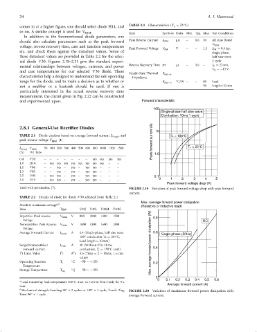
comes in at a higher ®gure, one should select diode H14, and TABLE 2.3 Characteristics (T L ¼ 25 C)
so on. A similar concept is used for V RRM . Item Symbols Units Min. Typ. Max. Test Conditions
In addition to the forementioned diode parameters, one
should also calculate parameters such as the peak forward Peak Reverse Current I RRM mA – 0.6 10 All class Rated
voltage, reverse recovery time, case and junction temperatures V RRM
Peak Forward Voltage V FM V – – 1.3 I FM ¼ 0:4 Ap,
etc. and check them against the datasheet values. Some of single-phase,
these datasheet values are provided in Table 2.2 for the selec- half sine wave
ted diode V 30. Figures 2.19–2.21 give the standard experi- 1 cycle
mental relationships between voltages, currents, and power Reverse Recovery Time trr ms – 3.0 – I F ¼ 22 mA,
and case temperatures for our selected V 30 diode. These V R ¼ÿ15 V
Steady-State Thermal R thðjÿaÞ
characteristics help a designer to understand the safe operating Impedance
range for the diode, and to make a decision as to whether or R thðjÿ1Þ C=W – – 80 Lead
not a snubber or a heatsink should be used. If one is 50 length¼10 mm
particularly interested in the actual reverse recovery time
measurement, the circuit given in Fig. 2.22 can be constructed
and experimented upon. Forward characteristic
100
Single-phase half sine wave
Conduction: 10ms 1 cycle
2.8.1 General-Use Rectifier Diodes (A) 10
current
TABLE 2.1 Diode election based on average forward current I FðavgÞ , and T = 150 C
L
°
peak inverse voltage V RRM [4]
forward T = 25 C
L
°
50 100 200 300 400 500 600 800 1000 1300 1500
I FðavgÞ V RRM
(A) (V) Type 1.0
Peak
0.4 V30 – – – – – – – yes yes yes yes
1.0 H14 – yes yes yes yes yes yes yes yes – –
1.1 V06 – – yes – yes – yes yes – – –
1.3 V03 – – yes – yes – yes yes – – –
2.5 U05 – yes yes – yes – yes yes – – – 0.1 0 1 2 3 4 5
3.0 U15 – yes yes – yes – yes yes – – –
Peak forward voltage drop (V)
Used with permission, [7]. FIGURE 2.19 Variation of peak forward voltage drop with peak forward
current.
TABLE 2.2 Details of diode for diode V30 selected from Table 2.1
Max. average forward power dissipation
Absolute maximum ratings a;b (Resistive or inductive load)
Item Type V30J V30L V30M V30N
Repetitive Peak reverse V RRM V 800 1000 1300 1500 0.8
Voltage DC
Nonrepetitive Peak Reverse V RSM V 1000 1300 1600 1800
Voltage
Average Forward Current I FðAVÞ A 0.4 (Single-phase, half sine wave 0.6 Single-phase (50Hz)
180 conduction TL ¼ 100 C,
Lead length ¼ 10 mm)
Surge(Nonrepetitive) I FSM A 30 (Without PIV, 10 ms Max. average forward power dissipation (W)
Forward current conduction, T j ¼ 150 C start) 0.4
2
2
2
I t Limit Value I t A s 3.6 (Time ¼ 2 10 ms, 1 ¼ rms
value)
Operating Junction T j C ÿ50 þ150 0.2
Temperature
Storage Temperature T stg c ÿ50 þ150
0
a Lead mounting: lead temperature 300 C max. to 3.2 mm from body for 5 s. 0 0.1 0.2 0.3 0.4 0.5 0.6
max. Average forward current (A)
b Mechanical strength: bending 90 2 cycles or 180 1 cycle, Tensile 2 kg, FIGURE 2.20 Variation of maximum forward power dissipation with
Twist 90 1 cycle. average forward current.