
Page 44 - Rashid, Power Electronics Handbook
P. 44
3 Thyristors 29
A high-resistivity region, n-base, is present in all thyristors. in the on-state). As long as the forward applied voltage does
It is this region, the n-base and associated junction J of Fig. not exceed the value necessary to cause excessive carrier
2
3.1, which must support the large applied forward voltages multiplication in the depletion region around J (avalanche
2
that occur when the switch is in its off- or forward-blocking breakdown), the thyristor remains in an off-state (forward-
state (nonconducting). The n-base is typically doped with blocking). If the applied voltage exceeds the maximum
impurity phosphorus atoms at a concentration of forward blocking voltage of the thyristor, it will switch to its
ÿ3
10 14 cm . The n-base can be 10s to 100s of mm thick to on-state. However, this mode of turn-on causes nonunifor-
support large voltages. High-voltage thyristors are generally mity in the current ¯ow, is generally destructive, and should
made by diffusing aluminum or gallium into both surfaces to be avoided.
obtain deep junctions with the n-base. The doping pro®le of When a positive gate current is injected into the device J
3
ÿ3
17
the p-regions ranges from about 10 15 to 10 cm . These p- becomes forward-biased and electrons are injected from the n-
regions can be up to 10s of mm thick. The cathode region emitter into the p-base. Some of these electrons diffuse across
(typically only a few mm thick) is formed by using phosphorus the p-base and are collected in the n-base. This collected
18
ÿ3
atoms at a doping density of 10 17 to 10 cm . charge causes a change in the bias condition of J . The
1
The higher the forward-blocking voltage rating of the change in bias of J causes holes to be injected from the p-
1
thyristor, the thicker the n-base region must be. However emitter into the n-base. These holes diffuse across the n-base
increasing the thickness of this high-resistivity region, results and are collected in the p-base. The addition of these collected
in slower turn-on and turn-off (i.e., longer switching times holes in the p-base acts the same as gate current. The entire
and=or lower frequency of switching cycles because of more process is regenerative and will cause the increase in charge
stored charge during conduction). For example, a device rated carriers until J also becomes forward biased and the thyristor
2
for a forward-blocking voltage of 1 kV will, by its physical is latched in its on-state (forward-conduction). The regenera-
construction, switch much more slowly than one rated for tive action will take place as long as the gate current is applied
100 V. In addition, the thicker high-resistivity region of the in suf®cient amount and for a suf®cient length of time. This
1 kV device will cause a larger forward voltage drop during mode of turn-on is considered to be the desired one as it is
conduction than the 100 V device carrying the same current. controlled by the gate signal.
Impurity atoms, such as platinum or gold, or electron irradia- This switching behavior can also be explained in terms of
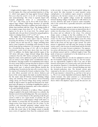
tion are used to create charge-carrier recombination sites in the two-transistor analog shown in Fig. 3.2. The two transis-
the thyristor. The large number of recombination sites reduces tors are regeneratively coupled so that if the sum of their
the mean carrier lifetime (average time that an electron or hole forward current gains (a's) exceeds unity, each drives the other
moves through the Si before recombining with its opposite into saturation. Equation 3.1 describes the condition necessary
charge-carrier type). A reduced carrier lifetime shortens the for the thyristor to move from a forward-blocking state into
switching times (in particular the turn-off or recovery time) at the forward-conduction state. The forward current gain
the expense of increasing the forward conduction drop. There (expressed as the ratio of collector current to emitter current)
are other effects associated with the relative thickness and of the pnp transistor is denoted by a , and that of the npn as
p
layout of the various regions that make up modern thyristors, a . The a's are current dependent and increase slightly as the
n
but the major trade-off between forward-blocking voltage current increases. The center junction J is reverse-biased
2
rating and switching times, and between forward-blocking under forward applied voltage (positive n ). The associated
AK
voltage rating and forward-voltage drop during conduction electric ®eld in the depletion region around the junction can
should be kept in mind. In signal-level electronics the analo-
gous trade-off appears as a lowering of ampli®cation (gain) to
achieve higher operating frequencies, and is often referred to
as the gain-bandwidth product. A A
The operation of thyristors is as follows. When a positive i A
voltage is applied to the anode (with respect to a cathode), the i A
thyristor is in its forward-blocking state. The center junction J 2 p
(see Fig. 3.1) is reverse-biased. In this operating mode the gate n n
current is held to zero (open-circuit). In practice, the gate
electrode is biased to a small negative voltage (with respect to p p G G
the cathode) to reverse-bias the GK-junction J and prevent
3
charge-carriers from being injected into the p-base. In this n i G i G
condition only thermally generated leakage current ¯ows K
through the device and can often be approximated as zero
in value (the actual value of the leakage current is typically K
many orders of magnitude lower than the conducted current FIGURE 3.2 Two-transistor behavioral model of a thyristor.