
Page 48 - Rashid, Power Electronics Handbook
P. 48
3 Thyristors 33
inductance within the module. Reducing the parasitic induc-
tance reduces the high-frequency ringing during transients
that is another cause of radiated electromagnetic interference,
as since stray inductance can cause large peak voltages during
switching transients, minimizing it helps to maintain the
device within its safe operating area.
Long life and high reliability are primarily attained through
minimization of thermal cycling, minimization of ambient
temperature, and proper design of the transistor stack. Ther-
mal cycling fatigues material interfaces because of coef®cient
of thermal expansion (CTE) mismatch between dissimilar
materials. As the materials undergo temperature variation,
they expand and contract at different rates, which stresses the
interface between the layers and can cause interface deteriora-
tion (e.g., cracking of solder layers or wire debonding).
Chemical degradation processes such as dendrite growth and
impurity migration are accelerated with increasing tempera-
ture, so keeping the absolute temperature of the device low
and minimizing the temperature changes to which it is subject
are important. Typical CTE values for common package
materials are given in Table 3.2.
Low cost is achieved in a variety of ways. Both manufactur-
ing and material costs must be taken into account when
designing a power module. Materials that are dif®cult to
machine or form, even if they are relatively cheap in raw
form, molybdenum, for example, should be avoided. Manu-
facturing processes that lower yield also drive up costs. In
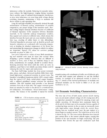
addition, a part that is very reliable can reduce future costs by FIGURE 3.7 Advanced module cut-away showing contacts without
reducing the need for repair and replacement. using wirebonds.
The basic half-bridge module has three power terminals:
plus, minus, and phase. Advanced modules differ from tradi-
tional high-power commercial modules in several ways. The manufacturing with attachment of shells, use of dielectric gels,
baseplate is metallized aluminum nitride (AIN) ceramic rather and with hard epoxies and adhesives to seal the ®nished
00
than the typical 0:25 -thick, nickel-plated copper baseplate module. An example of an advanced module is shown in
Fig. 3.7. Details of the thermal performance of modules and
with a soldered metallized ceramic substrate for electrical
advanced modules can be found in Beker et al. [4] and
isolation. This AlN baseplate stack provides a low thermal
Godbold et al. [5].
resistance from die to heat sink. The copper terminal power
buses are attached by solder to the devices in a wirebond-free,
low-inductance, low-resistance, device-interconnect con®g-
uration. The balance of the assembly is typical for module 3.4 Dynamic Switching Characteristics
The time rate of rise of both anode current (di=dt) during
TABLE 3.2 CTE for thyristor package materials turn-on and anode-cathode voltage (dn=dt) during turn-off is
an important parameter to control for ensuring proper and
Material CTE ðmm=m KÞ
reliable operation. All thyristors have maximum limits for
at 300 K
di=dt and dn=dt that must not be exceeded. Devices capable of
Silicon 4.1 conducting large currents in the on-state are necessarily made
Copper (baseplate and pole pieces) 17
AlN substrate 4.5 with large-surface areas through which the current ¯ows.
Al 2 O 3 (Alumina) 6.5 During turn-on, localized areas (near the gate region) of a
Tungsten (W) 4.6 device begin to conduct current. The initial turn-on of an SCR
Molybdenum (Mo) 4.9 is shown in Fig. 3.8. The cross section illustrates how injected
Aluminum (Al) 23 gate current ¯ows to the nearest cathode region, causing this
Metal matrix composites (MMC) 5–20
60=40 Solder (Pb=Sn eutectic) 25 portion of the npn transistor to begin conducting. The pnp
transistor then follows the npn into conduction such that