
Page 51 - Rashid, Power Electronics Handbook
P. 51
J. Hudgins et al.
3636 J. Hudgins et al.
Shorted cathode Fig. 3.9, right). When the gate current (1) is injected into the
Gate p-base through the pilot-gate contact, electrons are injected
p n + n + n + n + into the p-base by the n -emitter with a given emitter
þ
injection ef®ciency. These electrons traverse through the p-
base (time taken for this process is called the transit time) and
accumulate near the depletion region. This negative charge
n -
accumulation leads to injection of holes from the anode. The
device then turns-on after a certain delay, dictated by the p-
+
p p p p n -Region base transit time, and the pilot anode current (2 on the ®gure)
begins to ¯ow through a small region near the pilot-gate
contact as shown in Fig. 3.14.
Shorted anode This ¯ow of pilot anode current corresponds to the initial
FIGURE 3.13 Cross section showing integrated cathode and anode sharp rise in the anode current waveform (phase I), as shown
shorts. in Fig. 3.15. The device switching then goes into phase II,
during which the anode current remains fairly constant,
suggesting that the resistance of the region has reached its
so that the thyristor will remain in forward conduction when
lower limit. This is due to the fact that the pilot anode current
used with varying load impedances.
(2) takes a ®nite time to traverse through the p-base laterally
and become the gate current for the main cathode area. The
3.4.2 Anode Shorts n -emitters start to inject electrons which traverse the p-base
þ
vertically and after a certain ®nite time (transit time of the p-
A further increase in forward-blocking capability can be
base) reach the depletion region. The total time taken by the
obtained by introducing anode shorts (reduces a in a similar lateral traversal of pilot anode current and the electron transit
p
manner that cathode shorts reduce a ) along with the cathode time across the p-base is the reason for observing this
n
shorts. An illustration of this is provided in Fig. 3.13. In this
characteristic phase II interval. The width of the phase II
structure, both J and J are shorted (anode and cathode
3
1
shorts) so that the forward-blocking capability of the thyristor interval is comparable to the switching delay, suggesting that
is completely determined by the avalanche breakdown char- the p-base transit time is of primary importance. Once the
main cathode region turns on, the resistance of the device
acteristics of J . Anode shorts will result in the complete loss of
2 decreases and the anode current begins to rise again (transi-
reverse-blocking capability and is only for thyristors used in
tion from phase II to phase III). From this time onward in the
asymmetric circuit applications.
switching cycle, the plasma spreading velocity will dictate the
rate at which the conduction area will increase. The current
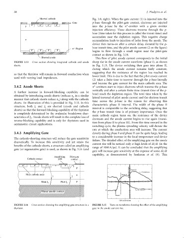
3.4.3 Amplifying Gate density during phase I and phase II can be quite large, leading
to a considerable increase in the local temperature and device
The cathode-shorting structure will reduce the gate sensitivity
failure. The detailed effect of the amplifying gate on the anode
dramatically. To increase this sensitivity and yet retain the
current rise will be noticed only at high levels of di=dt (in the
bene®ts of the cathode-shorts, a structure called an amplifying
range of 1000 A=ms). It can be concluded that the amplifying
gate (or regenerative gate) is used, as shown in Fig. 3.14 (and
gate will increase gate sensitivity at the expense of some di=dt
capability, as demonstrated by Sankaran et al. (8). This
Amplifying Pilot gate
Cathode contact gate contact
n + n + n + n + 1 p
I A 1.93 KA/division
Main cathode areas n
3 2
p
Main I A Pilot I A
Metal anode contact 0 V AK 500 V/division
100 ns/division
FIGURE 3.14 Cross section showing the amplifying gate structure in a FIGURE 3.15 Turn-on waveforms showing the effect of the amplifying
thyristor. gate in the anode current rise.